

Method for obtaining distribution of charges along channel in mos transistor
- Summary
- Abstract
- Description
- Claims
- Application Information
AI Technical Summary
Benefits of technology
Problems solved by technology
Method used
Image

Examples
Embodiment Construction
[0041]Hereinafter, a preferable embodiment will be described in more detail.
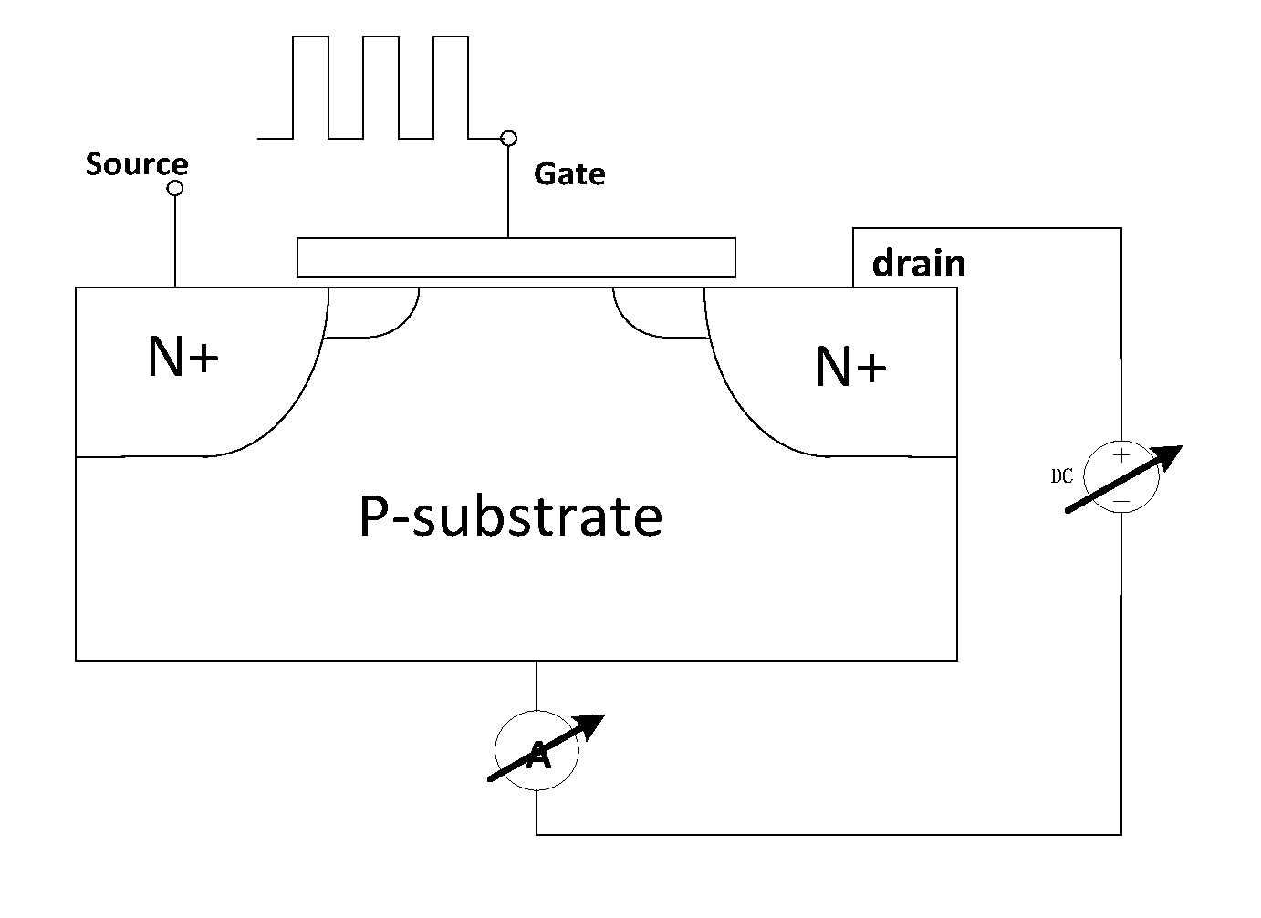
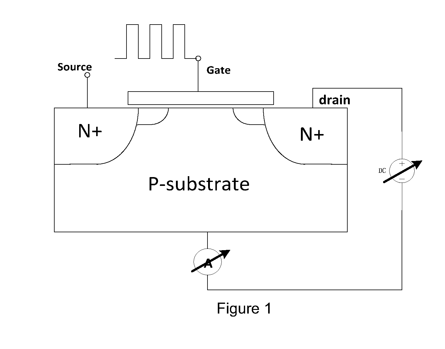
[0042]In the present embodiment, a MOS transistor to be tested is a NMOS transistor (similarly, the MOS transistor may be a PMOS transistor). A NMOS transistor having a width (W) of 6 μm and a length (L) of 0.5 μm, which has a good process condition and a uniform interface state, is used. After a hot carrier stress is biased for 1000 s, a test for charges of an interface state and charges of a gate dielectric layer of the transistor is performed. As shown in FIG. 1, a charge pumping current test method, in which one of a source terminal and a drain terminal is open-circuited and the other one is applied with a reverse-bias voltage, is used. A gate is applied with a pulse voltage which has a fixed frequency and a fixed magnitude, where the magnitude of the pulse voltage is larger than a difference between a threshold voltage Vth and a flat band voltage Vfb. Meanwhile, a base voltage is scanned, so that two cu...
PUM
 Abstract
Description
Claims
Application Information