Photomask blank, photomask, and making method

a technology of photomask and blank, applied in the field of photomask blank, photomask, and preparation of photomask, can solve problems such as processing errors, and achieve the effects of improving the resistance of hard mask film, high accuracy, and high ra

Active Publication Date: 2013-03-07
SHIN ETSU CHEM IND CO LTD
View PDF11 Cites 12 Cited by
  • Summary
  • Abstract
  • Description
  • Claims
  • Application Information

AI Technical Summary

Benefits of technology

[0025]The photomask blank of the invention is designed to enhance the resistance of a hard mask film to fluorine-based dry etching. Even on use of a thinner hard mask film, an optical film of material containing a transition metal and silicon can be processed at a high accuracy through the hard mask pattern.
[0026]Since the hard mask film is of multilayer construction, the hard mask film maintains its hard mask function during etching even when the low oxygen content layer of the hard mask film, which is difficult to etch at a high rate, is made thin. It is then possible to reduce the load applied to a resist film during processing of the hard mask film while maintaining the hard mask function against fluorine-based dry etching. This implies that the hard mask film can be processed at a high accuracy using a thinner resist film.
[0027]After the photomask blank is processed into a photomask by such patterning, the photomask is highly reliable on its use in the lithography of 32 nm node and below.

Problems solved by technology

As pointed out in Patent Document 1, a chromium-based material film if thick tends to undergo side etching when subjected to standard dry etching with oxygen-containing chlorine gas, and processing errors can occur due to the pattern density dependence or optical proximity effect.

Method used


Image

  • Photomask blank, photomask, and making method
  • Photomask blank, photomask, and making method
  • Photomask blank, photomask, and making method

Examples


example 1

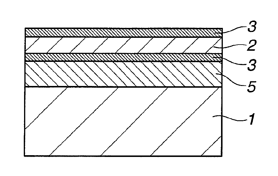
[0097]A light-side film of MoSiN consisting of a substrate-side compositionally graded layer and a surface-adjoining compositionally graded layer was deposited on a quartz substrate by a sputtering technique using a silicon target, a molybdenum silicide target, and argon and nitrogen gases as the sputtering gas. First, the substrate-side compositionally graded layer of 45 nm thick having an atomic ratio of Mo:Si=1:2.5 was deposited while continuously changing the nitrogen gas concentration so as to provide a nitrogen content of 29 atom % on the substrate side and a nitrogen content of 19 atom % on the side remote from the substrate. Subsequently, a sub-layer of 2 nm was deposited under such conditions as to provide an atomic ratio of Mo:Si=1:3.5 and a nitrogen content of 38 atom %, and another sub-layer of 2 nm was deposited under such conditions as to provide an atomic ratio of Mo:Si=1:3.5 and a nitrogen content of 47 atom %, yielding the surface-side compositionally graded layer c...

example 2

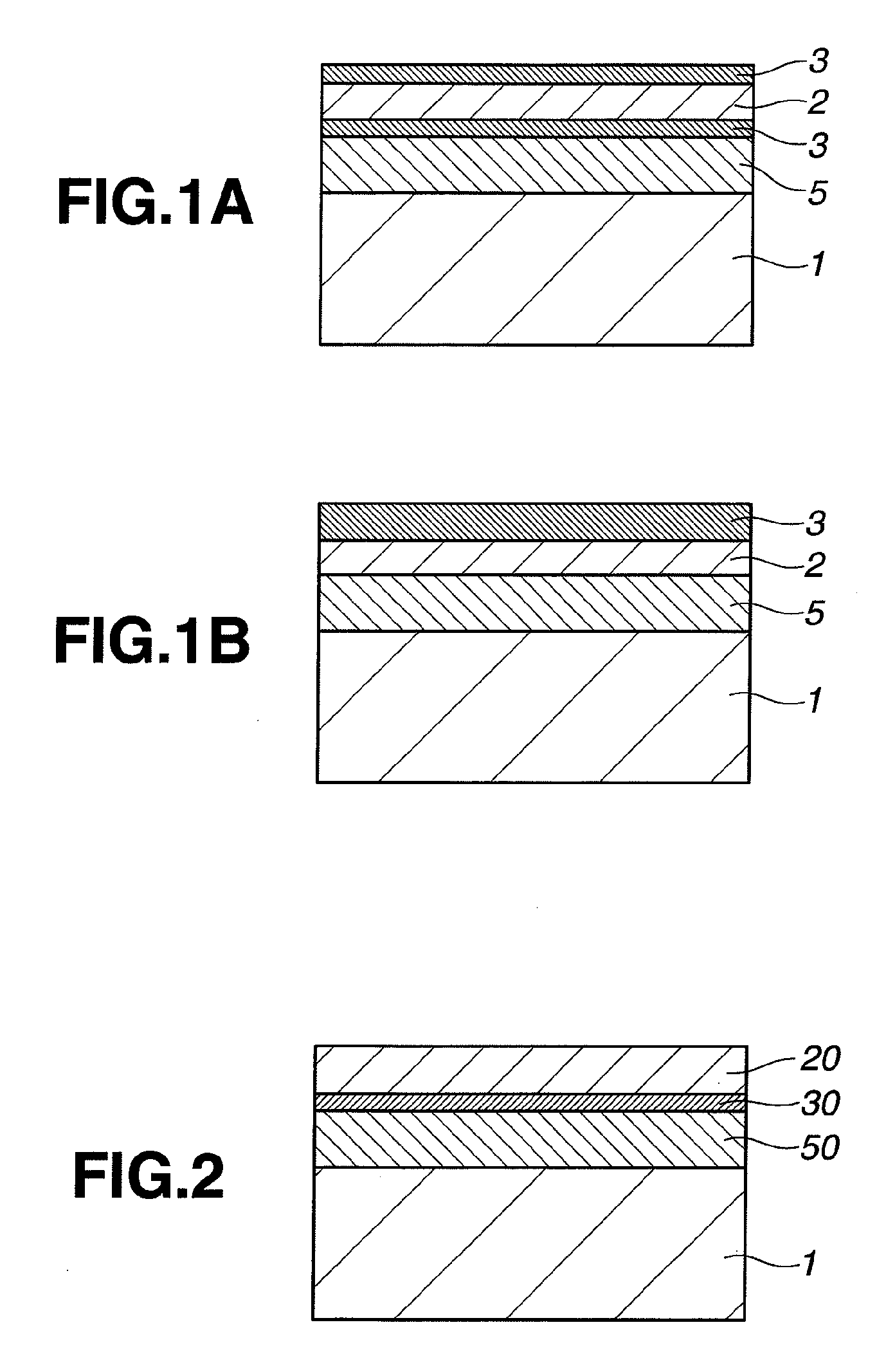
[0102]A binary photomask blank having a hard mask film was manufactured as in Example 1 except that the thickness of the lowermost, intermediate, and outermost layers was changed to 0.75 nm, 1.5 nm, and 0.75 nm, respectively.

example 3

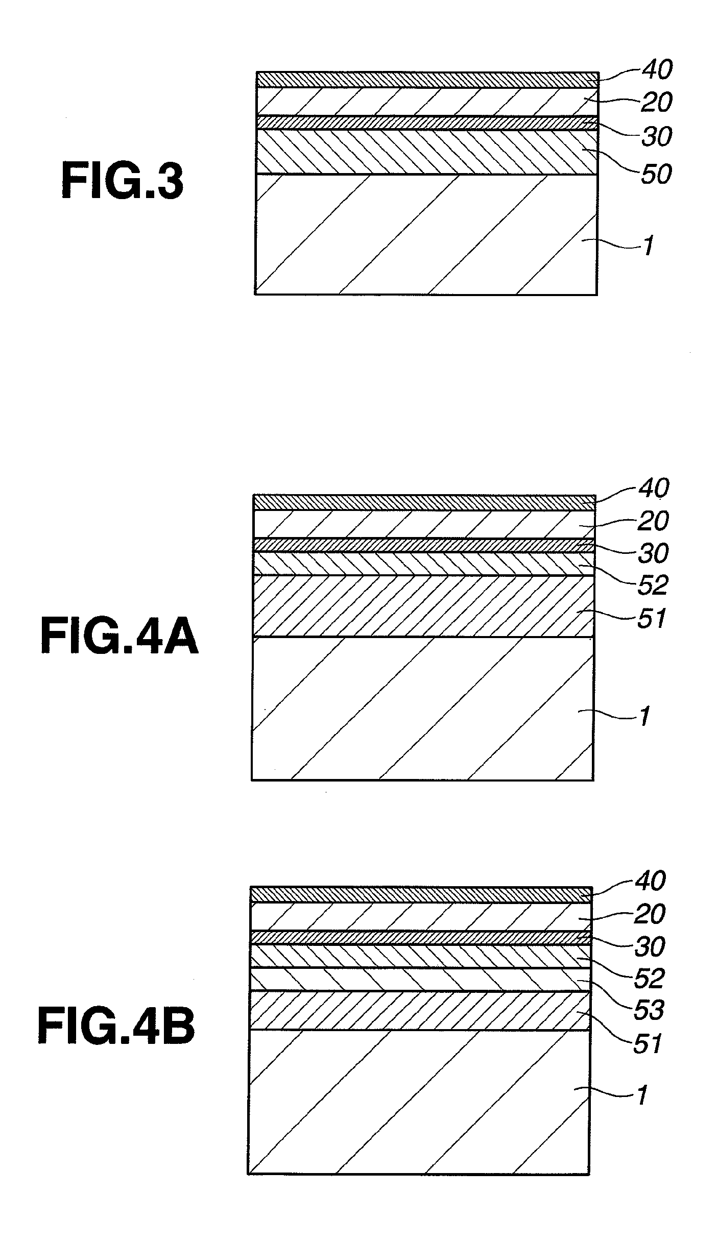
[0120]On the photomask blank prepared in Example 1, an ES lithography positive resist composition based on an aromatic polymer was coated to form a resist film of 80 nm thick, obtaining an EB resist film-covered photomask blank. A resist pattern including 45 nm and 400 nm line-and-space regions was formed therein as the photomask model pattern for 32 nm node. Specifically, the resist pattern was formed by using an EB mask writer system EBM-5000+ (Nuflare Technology, Inc.), writing a pattern including 45 nm and 400 nm line-and-space regions, baking and development in a standard way.

[0121]While the resulting resist pattern served as an etching mask, the hard mask film was etched under the chlorine dry etching conditions employed in the etching test of hard mask film. This transferred the resist pattern to the hard mask film, obtaining a hard mask pattern. While the resulting hard mask pattern served as an etching mask, the light-shielding film was etched under the fluorine dry etching...


PUM

PropertyMeasurementUnit
thicknessaaaaaaaaaa
thicknessaaaaaaaaaa
thicknessaaaaaaaaaa

Abstract

In a photomask blank comprising a transparent substrate, an optical film of material containing a transition metal and silicon, and a hard mask film, the hard mask film is a multilayer film including a first layer of a chromium-based material containing 20-60 atom % of oxygen and a second layer of a chromium-based material containing at least 50 atom % of chromium and less than 20 atom % of oxygen. The hard mask film having a thickness of 2.0 nm to less than 10 nm is resistant to fluorine dry etching.

Description

CROSS-REFERENCE TO RELATED APPLICATION[0001]This non-provisional application claims priority under 35 U.S.C. §119(a) on Patent Application No. 2011-195049 filed in Japan on Sep. 7, 2011, the entire contents of which are hereby incorporated by reference.TECHNICAL FIELD[0002]This invention relates to a photomask blank, a photomask, and preparation of the photomask. The photomask is used in the microfabrication of semiconductor integrated circuits, charge-coupled devices (CCD), liquid crystal display (LCD) color filters, magnetic heads or the like.BACKGROUND ART[0003]In the recent semiconductor processing technology, a challenge to higher integration of large-scale integrated circuits places an increasing demand for miniaturization of circuit patterns. There are increasing demands for further reduction in size of circuit-constructing wiring patterns and for miniaturization of contact hole patterns for cell-constructing inter-layer connections. As a consequence, in the manufacture of ci...

Claims


Application Information

Patent Timeline
Patent Type & Authority Applications(United States)
IPC IPC(8): G03F1/00G03F1/76G03F1/50B82Y30/00
CPCG03F1/14G03F1/50G03F1/38G03F1/26B82Y30/00G03F1/32G03F1/54G03F1/62G03F1/76G03F1/80H01L21/0273
Inventor INAZUKI, YUKIOIGARASHI, SHINICHINISHIKAWA, KAZUHIROYOSHIKAWA, HIROKI
Owner SHIN ETSU CHEM IND CO LTD
Why Eureka
Try Eureka