Fabricating method of NANO structure for antireflection and fabricating method of photo device integrated with antireflection NANO structure

a nanostructure and nano-structure technology, applied in the manufacture of microstructure devices, semiconductor devices, electrical devices, etc., can solve the problems of difficult to reduce the reflectance over a wide wavelength range and a wide incident angle, limited selection of coating materials used as anti-reflective layers, and complex processes. , to achieve the effect of good luminous efficiency and performance, short process time and low cos

Active Publication Date: 2013-03-28
GWANGJU INST OF SCI & TECH
View PDF10 Cites 18 Cited by
  • Summary
  • Abstract
  • Description
  • Claims
  • Application Information

AI Technical Summary

Benefits of technology

[0061]According to a method of fabricating a subwavelength nanostructure for anti-reflection and a method of fabricating a photo device integrated with a nanostructure for antireflection as described above, a solution containing a combination of metal ions with organic or inorganic ions may be coated on a substrate, the coated solution may be annealed using a sintering process to generate nanoscale metal particles, and a chemical etching process may be performed using the metal particles. As a result, the subwavelength nanostructure for antireflection may be fabricated without an apparatus requiring a vacuum state using a simple method for a short amount of process time. Thus, reflection of light generated between a semiconductor material and the air may be minimized, and the

Problems solved by technology

Although the refractive index and optical thickness of a coating material may be controlled using the ARC method to minimize a reflectance in a specific wavelength range, selection of a coating material used as an anti-reflective layer is limited according to the type of a semiconductor material.
Furthermore, it is difficult to reduce the reflectance over a wide wavelength range and a wide incident angle.
Although these processes do not cause disparity in etch rate according to a crystallization direction of a semiconductor substrate and enable a reduction in reflectance, the proce

Method used


Image

  • Fabricating method of NANO structure for antireflection and fabricating method of photo device integrated with antireflection NANO structure
  • Fabricating method of NANO structure for antireflection and fabricating method of photo device integrated with antireflection NANO structure
  • Fabricating method of NANO structure for antireflection and fabricating method of photo device integrated with antireflection NANO structure

Examples


embodiment 1

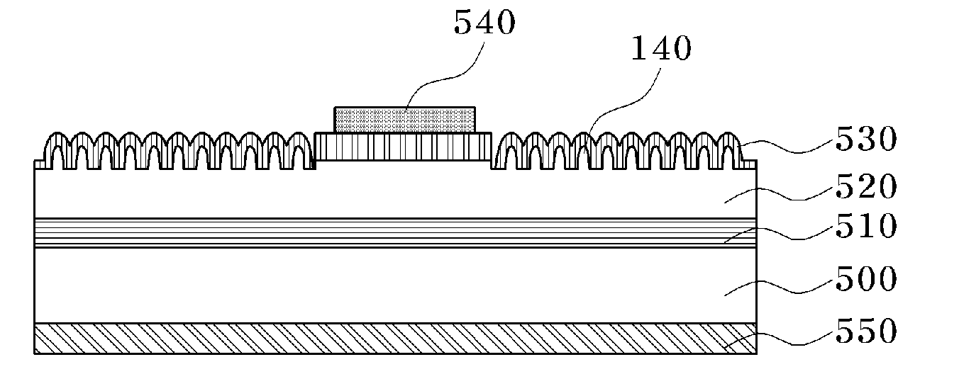
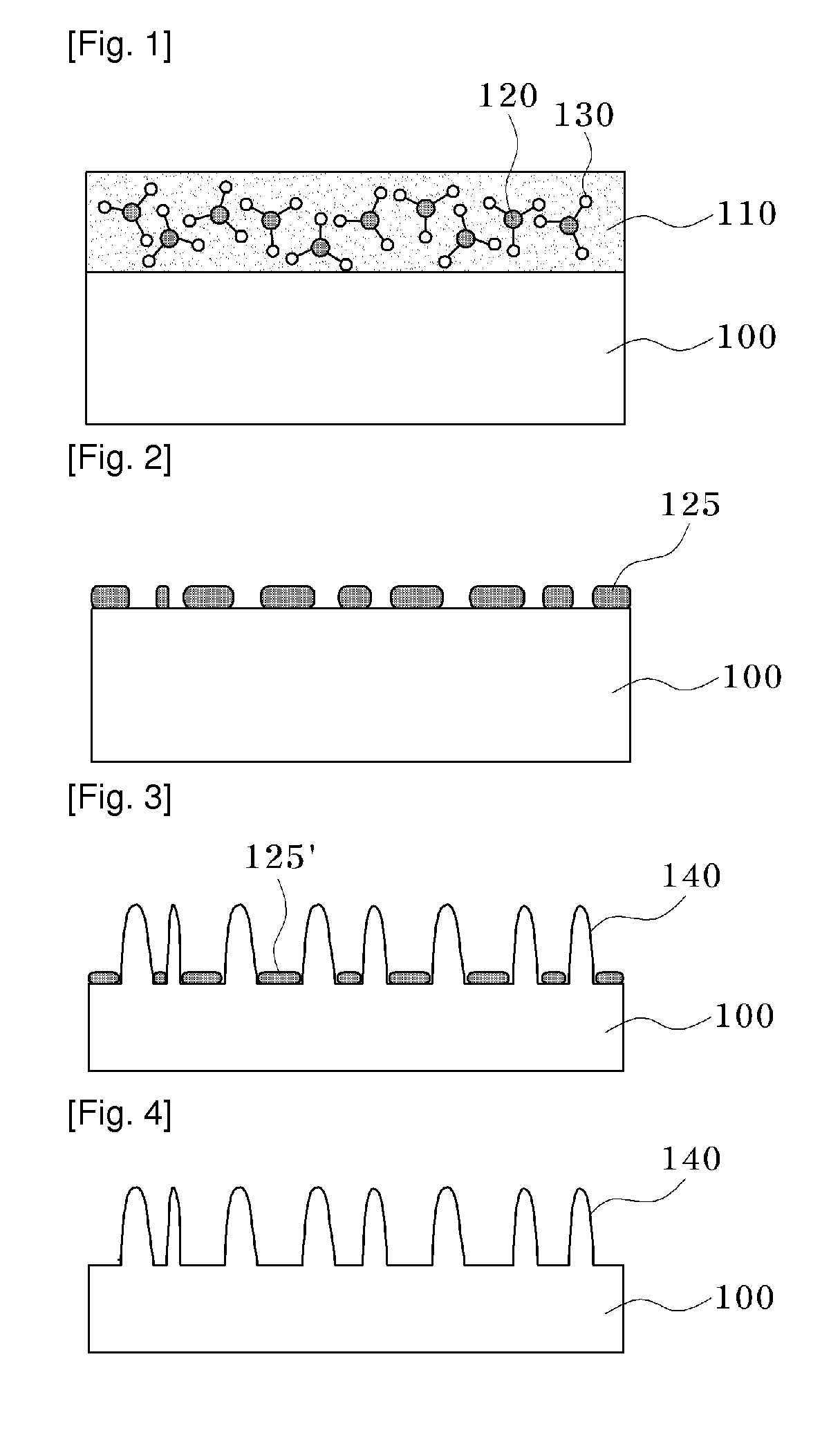
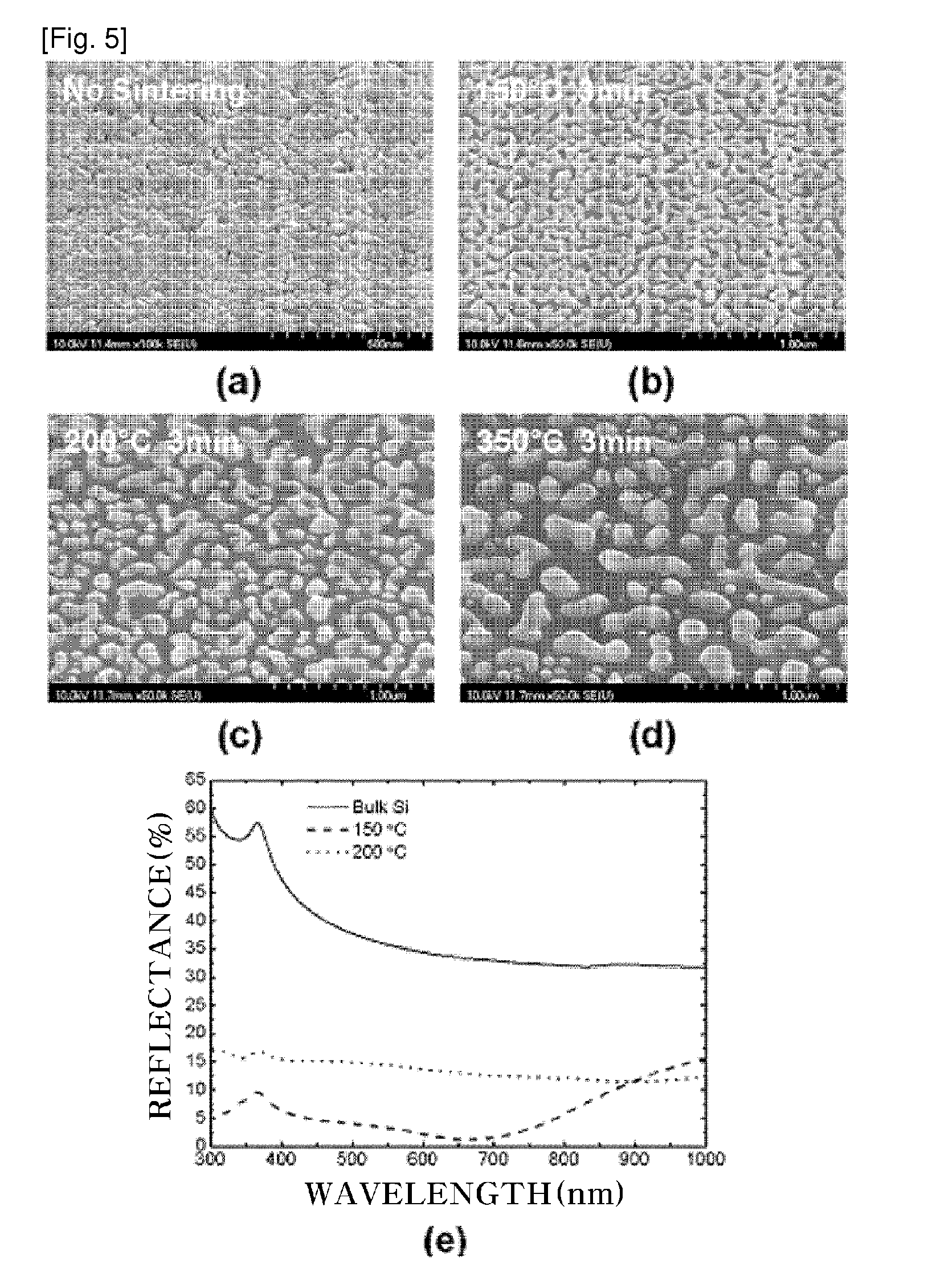
[0086]FIGS. 1 through 4 are cross-sectional views illustrating a method of fabricating a nanostructure for antireflection according to a first exemplary embodiment of the present invention.

[0087]Referring to FIG. 1, a solution 110 containing a combination of metal ions 120 with organic or inorganic ions 130 is uniformly coated on a top surface of a prepared semiconductor substrate 100.

[0088]For example, the substrate 100 may be a semiconductor substrate, which is not limited to a silicon (Si) substrate. Other than the semiconductor substrate, the substrate 100 may be any substrate that causes a reaction only in a portion containing metal particles (refer to 125 of FIG. 2) or accelerates the reaction in the portion containing the metal particles 125 more than the remaining portion because the metal particles 125 accelerate a chemical etching reaction.

[0089]Also, the metal ions 120 may be ions of any metal that may be bonded to the organic or inorganic ions 130 and contained in the so...

embodiment 2

[0134]FIGS. 17 through 20 are cross-sectional views illustrating a method of fabricating a nanostructure for antireflection according to a second exemplary embodiment of the present invention.

[0135]Referring to FIG. 17, a buffer layer 200 may be deposited on a top surface of a prepared substrate 100 using, for example, a plasma-enhanced chemical vapor deposition (PECVD) process, a thermal CVD process, or a sputtering process, and a solution 110 containing a combination of metal ions 120 with organic or inorganic ions 130 may be uniformly coated on the buffer layer 200.

[0136]Here, the substrate 100 may be a semiconductor substrate, which is not limited to a Si substrate. Other than the semiconductor substrate, the substrate 100 may be any substrate that allows deposition of the buffer layer 200 on a top surface of the substrate 100 and enables metal particles (refer to 125 of FIG. 18) to accelerate a chemical reaction more in a portion containing the metal particles 125 than in the r...

embodiment 3

[0147]FIGS. 21 through 24 are cross-sectional views illustrating a method of fabricating a nanostructure for antireflection according to a third exemplary embodiment of the present invention.

[0148]Referring to FIG. 21, a solution 110 containing a combination of metal ions 120 with organic or inorganic ions 130 is uniformly coated on a top surface of a prepared semiconductor substrate 100. For example, the substrate 100 may be a semiconductor substrate, which is not limited thereto. Other than the semiconductor substrate, the substrate 100 may be any substrate that causes no reaction in a portion containing metal particles (or metal grains) (refer to 125 of FIG. 22) during a chemical reaction using the metal particles as a mask.

[0149]Since FIG. 22 is the same as described in the first and second embodiments, a detailed description thereof will be omitted.

[0150]Referring to FIG. 23, for example, a chemical etching process may be performed on the top surface of the substrate 100 contai...


PUM


Abstract

A method of fabricating nanostructure for antireflection and a method of fabricating a photo device integrated with the nanostructure for antireflection are provided. The fabrication of the nanostructure for antireflection includes coating a solution containing a combination of metal ions with organic or inorganic ions on a substrate, sintering the coated solution using an annealing process to grow nanoscale metal particles, and chemically etching the substrate using the metal particles as mask or accelerator to form a subwavelength nanostructure on the surface of the substrate, thereby manufacturing the nanostructure for antireflection without an apparatus requiring a vacuum state using a simple method for a short amount of time to minimize reflection of light at an interface between a semiconductor material and the air, and producing a photo device having good luminous efficiency and performance at low cost in large quantities by applying it to the photo device.

Description

TECHNICAL FIELD[0001]The present invention relates to a method of fabricating a nanostructure for anti-reflection and a method of fabricating a photo device integrated with an anti-reflection nanostructure, and more particularly, to a method of fabricating a nanostructure for anti-reflection, which includes coating a solution containing a combination of metal ions with organic or inorganic ions on a substrate, sintering the coated solution using an annealing process to grow nanoscale metal particles, chemically etching the substrate using the sintered nanoscale metal particles so that a subwavelength nanostructure for antireflection may be formed on the semiconductor substrate for a short amount of process time using a simple method without an apparatus requiring a vacuum state. Thus, the nanostructure for antireflection may minimize reflection of light at an interface between a semiconductor material and the air. Also, the nanostructure for anti-reflection may be integrated with a ...

Claims


Application Information

Patent Timeline
IPC IPC(8): H01L33/00
CPCB81C1/00031H01L33/005H01L33/22
Inventor YEO, CHAN ILLEE, YONG TAKSONG, YOUNG MIN
Owner GWANGJU INST OF SCI & TECH
Why Eureka
Try Eureka