Ultraviolet laser

a laser and ultraviolet light technology, applied in semiconductor lasers, instruments, other domestic objects, etc., can solve the problems of high driving voltage, short operating life and long warm-up time, toxic materials in mercury lamps, etc., and achieve the effect of reducing the wavelength range of ligh

Inactive Publication Date: 2013-04-25
SHARP KK
View PDF10 Cites 10 Cited by
  • Summary
  • Abstract
  • Description
  • Claims
  • Application Information

AI Technical Summary

Benefits of technology

[0017]An advantage of using a UV laser made by frequency doubling is that the device can emit both the UV laser light and a portion of the visible laser light. The visible laser light beam is particularly useful from a safety point of view, since (unlike deep UV light) it is visible to the naked eye.
[0031]g) The use of highly collimated and tightly focused laser beams for fast and effective treatment and achieving high sensing signals from airborne or waterborne micro-organisms.

Problems solved by technology

However, mercury lamps contain toxic material, tend to have short operating lifetimes and long warm-up times and require high driving voltages.
Furthermore, the UV light emitted from mercury lamps is emitted in a broad range of directions and from a relatively large area which means it cannot be efficiently focused into a small area or a collimated beam.
The current draw-backs to using UV LEDs include that they have short operating lifetimes and that they cannot be efficiently focused to provide a collimated beam or tightly focused light spot.
In addition, the performance of UV LEDs with emission wavelengths shorter than 260 nm is very poor.
Therefore, these devices are poorly suited for the applications described above which benefit from a light source with wavelength shorter than 260 nm.
However, existing lasers with emission wavelengths shorter than 280 nm are very expensive components such as gas lasers designed for industrial use.
However, the SHG process in BBO occurs with low efficiency for the relatively low powers of light emitted from blue-violet semiconductor laser diodes.
Consequently, although a complex optical system was used to recirculate the blue light through the BBO component to improve efficiency, the UV output power achieved in this prior art was still low.
Therefore, this method is not suitable to fabricate a low-cost high-power UV light source for the applications described above.
This prior art does not use a visible laser diode nor BBO as the FD waveguide material so does not provide a method to make a UV laser.
In particular, there is no method known in the prior art to deposit high-quality single crystal BBO thin films onto substrates, other than homoepitaxial deposition onto BBO substrates which provide no refractive index contrast with the deposited BBO layer as required for a waveguide.
Therefore, this method is not suitable to fabricate a high-quality waveguide for a deep UV laser.
This prior art does not discuss the use of BBO, nor any other nonlinear material suitable for frequency-doubling to deep UV wavelengths, and it is not clear that diffusion can be used to form high-quality waveguides suitable for use in a deep UV laser.
Furthermore, this prior art does not provide cladding layers with composition significantly different from that of the non-linear crystal, as is required to make a waveguide where the light is strongly confined.
The latter reports on using BBO but none of them provide cladding layers with composition significantly different from that of the non-linear crystal.
Furthermore, these methods for fabrication a waveguides tend to result in high absorption losses for ultraviolet light with very short wavelength (e.g. wavelength less than 280 nm).
However, there is no method known in the prior art to deposit high-quality single crystal BBO thin films onto substrates, other than homoepitaxial deposition onto BBO substrates which provide no refractive index contrast with the deposited BBO layer as required for a waveguide.
Therefore, this method is not suitable to fabricate a high-quality waveguide for a deep UV laser.
There are significant disadvantages to using implantation to form the waveguide.
In particular, the refractive index contrast between the implanted layer and the BBO crystal is relatively weak, which means light can “leak” out of the waveguide, the BBO crystal between the implanted layer and the surface is damaged during the implantation process and this reduces the UV output power, and absorption losses for ultraviolet light with very short wavelength (e.g. wavelength less than 280 nm) tend to be high.
The visible laser used with the waveguide in this prior art was a bulky and expensive industrial laser which is a further disadvantage of this method.
Consequently, a BBO thin film fabricated according to the proposal in this prior art will have high absorption losses of the UV laser wavelength and therefore provide low efficiency.
Furthermore, the absorption of the deep UV light will likely contribute to degradation of the material and result in a short lifetime of the waveguide component.

Method used


Image

  • Ultraviolet laser
  • Ultraviolet laser
  • Ultraviolet laser

Examples


example 1

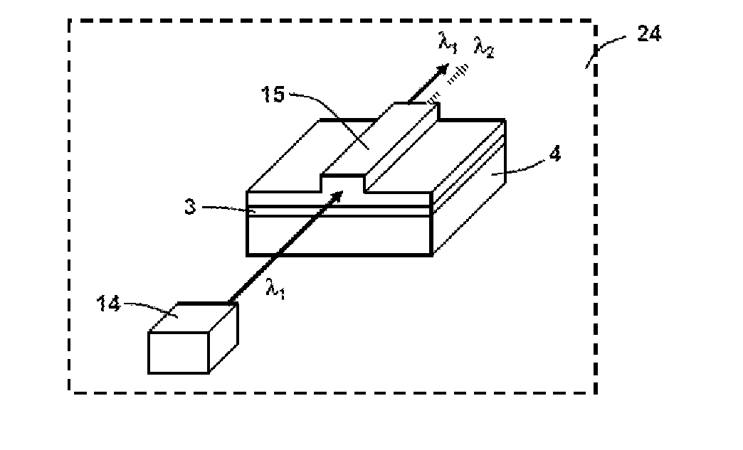
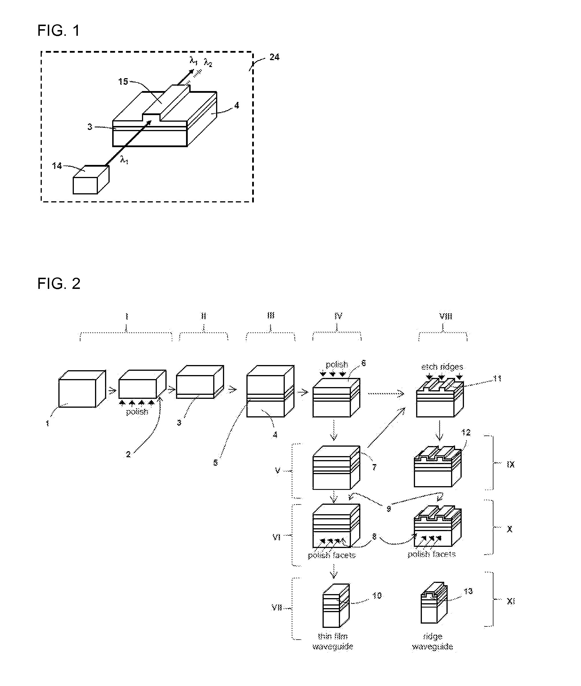
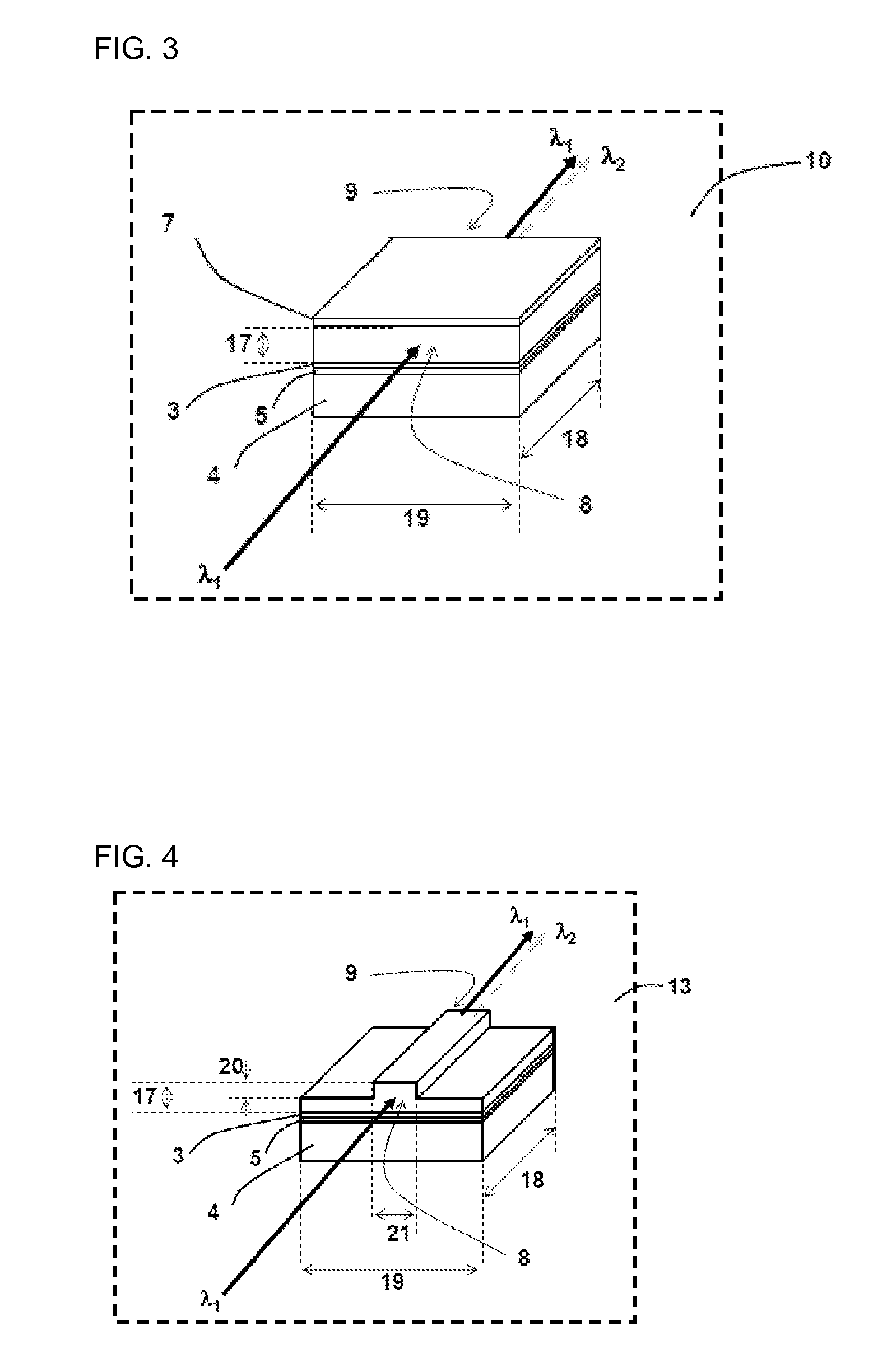
[0137]The first embodiment of the present invention is now described. The laser device 24, illustrated in FIG. 6, comprises of a semiconductor laser diode 14 to generate a visible laser light with a wavelength, λ1, in the range 400-560 nm which is coupled into a frequency doubling crystal of BBO taking the form of a single crystal thin film ridge waveguide structure 15. λ1 is preferably in the range from 410 nm to 460 nm. The light is coupled from the laser diode 14 to the waveguide 15 using one or more lenses 16 which collect the light emitted from the laser diode 14 and focus the light into the waveguide 15. Preferably, the dominant polarization of the light entering the waveguide has the electric field perpendicular to the interface between the BBO crystal (e.g., the single crystal nonlinear optical material) and the first cladding layer. A portion of the visible light from the semiconductor laser diode is frequency-doubled in the waveguide to generate light with wavelength λ2=λ1...

example 2

[0141]A second embodiment of the present invention is now described. The laser device 24, illustrated in FIG. 8, comprises of a semiconductor laser diode14 to generate a visible laser light with a wavelength, λ1, in the range 400-560 nm which is coupled into a frequency doubling crystal of BBO taking the form of a single crystal thin film planar waveguide structure 22. λ1 is preferably in the range from 410 nm to 460 nm. The light is coupled from the laser diode 14 to the waveguide 22 using one or more lenses 23 which collect the light emitted from the laser diode 14 and focus the light into the waveguide 22. Preferably, the dominant polarization of the light entering the waveguide has the electric field perpendicular to the interface between the BBO crystal (e.g., the single crystal nonlinear optical material) and the first cladding layer. A portion of the visible light from the semiconductor laser diode is frequency-doubled in the waveguide to generate light with wavelength λ2=λ1 / ...

example 3

[0142]A third embodiment of the present invention is now described. The laser device is the same as described for Example 1 except for the orientation of the BBO wafer used in step I of the waveguide fabrication. In this embodiment a single crystal BBO wafer 1 with typical dimensions of 9 mm×9 mm×0.5 mm (or other dimensions as required for the particular application) is used as the nonlinear optical single crystal. The BBO wafer has a BBO crystal direction less than 5° from the direction perpendicular to its principal surfaces (that is the 9 mm×9 mm surfaces) and has the BBO [0001] crystal direction lying in the plane of its principal surfaces. The plane of the first polished surface 2 is less than 5° away from being parallel to a {1-100} lattice plane of the BBO crystal (0° is preferred). The approximate relationship between the crystal directions and the first polished surface 2 of the BBO wafer 1 is indicated in FIG. 9. Commercially available BBO wafers may be sourced with the {...


PUM

PropertyMeasurementUnit
wavelengthaaaaaaaaaa

Abstract

A laser device is disclosed that provides at least an ultraviolet laser beam and preferably both an ultraviolet laser beam and a visible laser beam. The laser device includes a semiconductor laser device (e.g. a laser diode) to generate visible laser light which is coupled into a frequency doubling crystal taking the form of a single crystal thin film frequency-doubling waveguide structure. The single crystal thin film frequency-doubling waveguide converts a portion of the visible light emitted by the laser diode into ultraviolet light. Both visible and ultraviolet laser light is emitted from the waveguide. As an example, the single crystal thin film frequency-doubling frequency doubling waveguide includes a frequency doubling crystal region composed of β-BaB2O4 (β-BBO), a cladding region composed of materials that are transparent or nearly transparent at the wavelength of the ultraviolet laser light beam and a supporting substrate composed of any material.

Description

TECHNICAL FIELD[0001]The present invention relates to a device for the emission of ultraviolet laser light and more particularly to a device with a frequency doubling waveguide type optical component for converting visible laser light into ultraviolet laser light and a process for manufacturing the frequency doubling waveguide. The device may be used as the light source in products designed for the germicidal treatment of water.BACKGROUND ART[0002]There is an ever increasing need for clean and safe air to breathe and water to drink, particularly in heavily populated countries or regions throughout the world. A major, high-volume, application for compact solid-state deep UV light sources is for chemical-free sterilisation of air or water. Deep UV light—that is light in the UVC range which has wavelength shorter than 280 nm—efficiently causes permanent physical damage to DNA which prevents bacteria, viruses and fungi from replicating. This means that deep UV treatment can be used to d...

Claims


Application Information

Patent Timeline
Patent Type & Authority Applications(United States)
IPC IPC(8): H01S5/10B05D5/06B29D11/00
CPCG02F1/3551G02F1/377C02F2303/04C02F2201/3222C02F2201/3226C02F1/325G02B2006/12097G02F1/353H01S5/026H01S5/0605
Inventor SMEETON, TIMHOOPER, STEWARTBOARDMAN, EDWARD ANDREWCOLE, ROBIN MARK
Owner SHARP KK
Why Eureka
Try Eureka