Sinterable bonding material using copper nanoparticles, process for producing same, and method of bonding electronic component

a technology of sinterable bonding material and copper nanoparticles, which is applied in the direction of non-conductive materials with dispersed conductive materials, printed circuit assembling, solid-state devices, etc., can solve the problems of difficult sintering in atmospheric air, difficult low-temperature sintering per se, and oxidized copper. oxidation and the effect of bondability

Inactive Publication Date: 2013-05-02
HITACHI LTD
View PDF11 Cites 23 Cited by
  • Summary
  • Abstract
  • Description
  • Claims
  • Application Information

AI Technical Summary

Benefits of technology

[0019]According to the present invention, the oxidation resistance and the bondability of the sinterable bonding material using the copper nanoparticles can be rendered compatible and ion migration in the bonding portion of a semiconductor device or the like manufactured by using the sinterable bonding material can be suppressed.

Problems solved by technology

However, silver involves a drawback of tending to cause ion migration which tends to cause short-circuit.
However, cleaning of the copper nanoparticles involves a problem that metallic copper is oxidized into cuprous oxide.
Once the metallic copper is oxidized into cuprous oxide, sintering in atmospheric air becomes difficult.
Therefore, low temperature sintering per se is difficult.
It is considered that the copper powders described in Patent Document 1 and Patent Document 2 are excellent in the oxidation resistance, but it may be a possibility that the residue of the silicone oil tends to be left in the bonded portion upon sintering heat treatment in a narrow space for such an application as bonding electronic components to each other, thereby deteriorating the bonding strength or thermal conductivity.
The electroconductive composition may have difficulties in uniform coating to the nanoparticles having a particle diameter of 100 nm or less, and suppression of oxidization of the nanoparticles.

Method used


Image

  • Sinterable bonding material using copper nanoparticles, process for producing same, and method of bonding electronic component
  • Sinterable bonding material using copper nanoparticles, process for producing same, and method of bonding electronic component
  • Sinterable bonding material using copper nanoparticles, process for producing same, and method of bonding electronic component

Examples


example 1

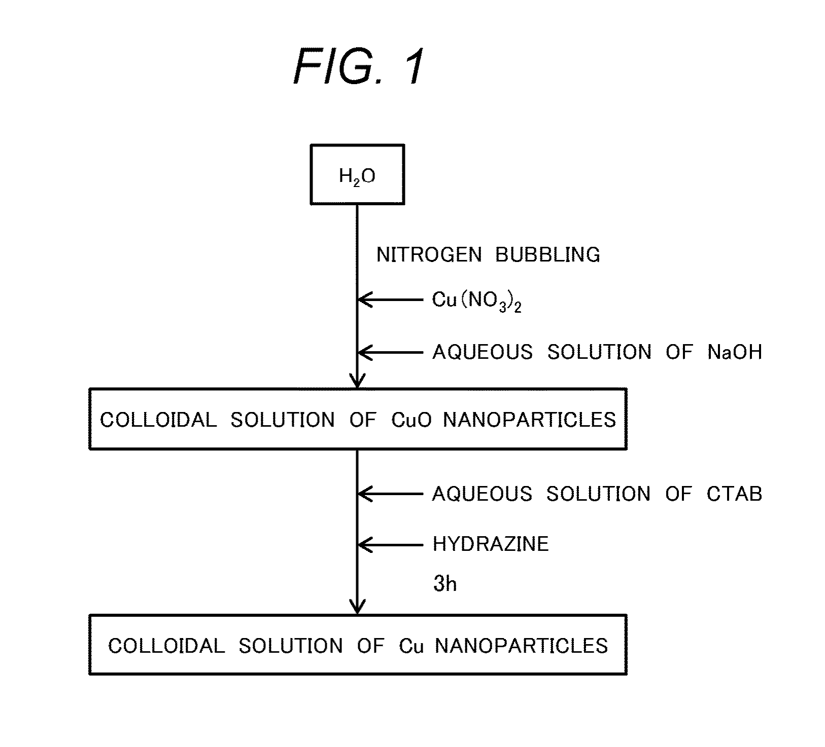
(Preparation of Copper Nanoparticles)

[0103]As a starting compound for copper, a powder of Cu (NO3)2.3H2O was used, water was used as a solvent. NaOH was used as a precipitating agent of cupric oxide nanoparticles. 1.932 g of a powder of Cu(NO3)2.3H2O was added to 784.8 mL of distilled water subjected to nitrogen bubbling for 30 minutes in a beaker of 1,000 mL volume, and the powder was dissolved uniformly in a water bath at 20° C. and 80° C. Then, by dropping 15.2 mL of a 1.0 M aqueous solution of NaOH, a colloidal liquid dispersion of cupric oxide nanoparticles was prepared.

[0104]Then, after stirring the colloidal liquid dispersion of cupric oxide nanoparticles at a room temperature for 24 hours, 1.82 g of CTAB was dissolved in 190.3 mL of water, to which 9.7 mL of hydrazine was dropped to prepare a colloidal liquid dispersion of copper nanoparticles.

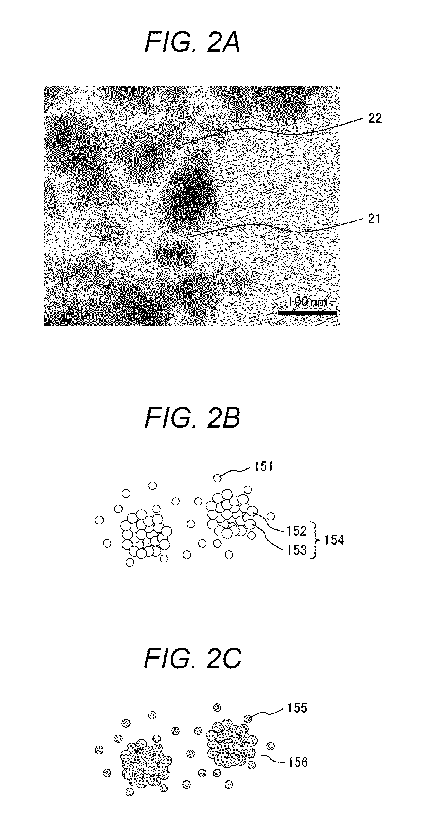
[0105]The obtained copper nanoparticles were subjected to centrifugal separation (centrifugal cleaning machine, Suprema 21 manufactur...

example 2

(Bonding Strength Test on Sinterable Bonding Material)

[0119]A bonding strength test was performed while simulating bonding between electronic components to each other. The test method is as shown below.

[0120]As a copper specimen for measurement, a lower test specimen of 10 mm diameter and 5 mm thickness and an upper test specimen of 5 mm diameter and 2 mm thickness were used. The sinterable bonding material was coated on the upper surface of the lower test specimen and dried at 80° C. under a reduced pressure for one hour. Subsequently, the upper test specimen was placed over the dried sinterable bonding material. A sintering heat treatment was performed in hydrogen at a temperature of 400° C. for 5 minutes while simultaneously applying a load at a surface pressure of 1.2 MPa to obtain a bonded test specimen.

[0121]A shear stress was loaded on the bonded test specimen by using a shear tester (Bond tester SS-100KP, maximum load 100 kg, manufactured by Nissin Shoji Co.) (shear rate: 30...

example 3

(Application to Cooling Unit)

[0126]Description is to be made to an example of using a sinterable bonding material of the present invention for pin connection of a pin fin cooling unit of a semiconductor power module.

[0127]In the semiconductor power module, since the amount of heat generation have tended to be increased in recent years, a technique of efficiently dissipating the heat generated during operation to the outside of the module has become important more and more.

[0128]FIG. 6 is a schematic cross sectional view showing an example of a wiring substrate and a pin fin cooling unit used in a semiconductor power module.

[0129]As shown in the drawing, a wiring substrate 14 has a structure of stacking a circuit wiring 11 to be connected with a semiconductor chip, an insulation substrate 12 for electrically insulating a semiconductor chip and the circuit wiring 11 in the inside of a module, and a metallized layer 13 for soldering the insulation substrate 12 and the pin fin cooling u...


PUM

PropertyMeasurementUnit
particle diameteraaaaaaaaaa

Abstract

Disclosed is a sinterable bonding material which is a liquid or a paste containing copper nanoparticles having a particle diameter of 1,000 nm or less, in which the copper nanoparticles have one or more particle diameter peaks of a number-based grain size distribution within a class of particle diameter of 1 to 35 nm and within a class of particle diameter of more than 35 nm and 1,000 nm or less respectively, and in which the copper nanoparticles include individual particles (primary particles) and secondary particles, each of the secondary particles being a fused body of the primary particles. Thus, oxidation resistance and bondability are made compatible in a sinterable bonding material using copper nanoparticles, and ion migration is suppressed in a bonded portion of a semiconductor device, etc. manufactured by using the sinterable bonding material.

Description

CLAIM OF PRIORITY[0001]The present application claims priority from Japanese Patent application serial No.2011-235605, filed on Oct. 27, 2011, the content of which is hereby incorporated by reference into this application.BACKGROUND OF THE INVENTION[0002]1. Field of the Invention[0003]The present invention concerns a sinterable bonding material using copper nanoparticles, a process for producing the same, and a method of bonding electronic components by using the sinterable bonding material.[0004]2. Description of Related Art[0005]Since metal nanoparticles (having a particle diameter of 100 nm or less, for example) have a large specific surface area relative to the volume of a particle, they have high chemical activity and have extremely low sintering temperature. Due to the property, the metal nanoparticles have attracted attention as a novel functional material. For example, a paste containing the metal nanoparticles is expected as a material used for bonding electronic components...

Claims


Application Information

Patent Timeline
Patent Type & Authority Applications(United States)
IPC IPC(8): B23K35/24H01L23/488B23K31/02B22F1/054
CPCH01L2224/16225H01B1/22H05K1/097H05K3/32H05K2201/0266H01B1/026B82Y30/00B22F3/10B22F9/24C22C1/0425B22F1/0018C22C9/00H01L2224/8384H01B1/16H01L2224/83205B22F1/054B22F1/056H01L2924/00014
Inventor YASUDA, YUSUKEMORITA, TOSHIAKIKOBAYASHI, YOSHIO
Owner HITACHI LTD
Why Eureka
Try Eureka