Nanoantenna arrays for nanospectroscopy, methods of use and methods of high-throughput nanofabrication

a nanoantenna array and nanotechnology, applied in the field of nanoantenna arrays, can solve the problems of weak absorption signals, limited signal enhancement factors in the 10-100 range, and inability to reproduce vibrational measurements, etc., to achieve enhanced ir absorption (ceira), high reliability and reproducibility, and long plasmon lifetimes

Active Publication Date: 2013-06-13
TRUSTEES OF BOSTON UNIV
View PDF4 Cites 219 Cited by
  • Summary
  • Abstract
  • Description
  • Claims
  • Application Information

AI Technical Summary

Benefits of technology

[0009]One aspect of the present invention relates to nanoantenna arrays comprising a plurality of nanostructures arranged in a predefined pattern for collective excitement of surface plasmons. Another aspect of the present invention described herein relates in part, to nanostencils and methods of fabricating complex plasmonic nanoantenna arrays, for example nanoantenna arrays comprising plasmonic or non-plasmonic nanostructures. By enabling optical and electrical signal transmission through the same metal circuitry, nanoplasmonics using the devices and methods described herein can lead to large scale on-chip integration of electronic and photonic components with high-fidelity.
[0012]Thus, the inventors have demonstrate herein that nanostructures, e.g., plasmonic nanostructures of a predefined shape and a pre-defined pattern results in a collective resonant excitation. Accordingly, in the nanoantenna arrays as disclosed herein comprise nanoantennas (or plasmonic nanostructures) which have predefined shapes and are organized on the nanoantenna array in a predefined pattern (as opposed to configured at random), to result in radiative dipolar coupling and the interference of the multiple scattering from antennas in the array can be utilized for the spectral narrowing of the far field response. These collective resonances are linked to the strongly enhanced near-field intensities, and can be used for a much stronger or enhanced coupling between the incident field and the transition dipole moments of the proteins as compared to the individual nanoantennas, randomly organized nanoantennas or chemically prepared supports.
[0013]Accordingly, the present invention relates to a method of use of the nanoantenna arrays for an ultra-sensitive collectively enhanced IR absorption (CEIRA) spectroscopy technique, allowing direct identification of vibrational signatures of single proteins and protein monolayers, for example, silk fibroin. Measurement of vibrational signatures with zepto-mole level protein detection limits are achieved due to the 104-105 signal enhancements, demonstrating the use of the nanoantenna arrays for nanospectroscopy. Absorption signals for the nanostructures on the nanoantenna arrays as disclosed herein are demonstrated herein with high reliability and reproducibility and far surpass those of the individual nanostructures by themselves.
[0014]Additionally, the inventors have also surprisingly discovered that significantly longer plasmon lifetimes and stronger near-field enhancements can be achieved by embedding the plasmonic nanostructures, such as nanoantennas into the support of the nanoantenna array. The inventors demonstrated that embedding the plasmonic nanostructures, such as the nanoantennas are in the same plane, or below the surface of the support (e.g., depressed or in a recess) results in a more homogeneous dielectric background, allowing stronger diffractive couplings among plasmonic particles leading to strong suppression of the radiative damping. Using embedded plasmonic nanostructures results in near-field enhancements well beyond than those achievable with isolated nanoparticles. Such nanoantenna arrays, including those with raised (e.g., on-surface), or embedded plasmonic nanostructures enhances electromagnetic fields obtained in these structures and are useful for biosensing and non-linear photonics applications.
[0050]Another aspect of the present invention provides for high-throughput fabrication of a nanoantenna array which has optical qualities comparable or superior to that of nanoantenna arrays fabricated by other means, for example, electron beam lithography. In some embodiments, the methods and processes for high-throughput fabrication of nanoantenna arrays involves nanostencil lithography (NSL) fabrication methods, enabling nanostructures (of plasmonic or non-plasmonic materials) of predefined shapes to be arranged in predefined patterns, e.g., in organized or a periodic array configuration. In addition, the nanostencil masks as described herein for the nanofabrication processes according to the invention can be reused many times to fabricate many series of nanostructures, or complex nanoantenna arrays with identical optical responses at a relatively low cost. Furthermore, the processes according to the invention provide the flexibility and the resolution to create complex plasmonic nanostructures on supports that are difficult to produce using e-beam and ion beam lithography tools. The inventors have shown that large field enhancements in nanoplasmonics can lead to ultra-sensitive infrared spectroscopy and have shown detection of vibrational signatures of proteins at zepto-mole sensitivity levels (Adato, R et al., PNAS 2009, 106, 46, 19227-19232)
[0062]Other aspects provide novel plasmonic structures, e.g., nanoantenna arrays, fabricated according to any of the methods of depositing a plurality of plasmonic nanostructures on a support described herein. In some embodiments, the support of the plasmonic structures, e.g., nanoantenna arrays, fabricated according to the methods described herein comprise a support, for example, where the support is non-conducting material. In some embodiments, the support allows nanostructures to be embedded or attached to the surface of the support, where the nanostructures, e.g., nanoantenna arrays can comprise a conducting material, a non-conducting material, or a magnetic material. In some such embodiments, the conducting material comprises silicon. In some embodiments, the non-conducting material comprises glass, quartz, or calcium fluoride (CaF2).

Problems solved by technology

In these supports, however, signal enhancement factors have been limited to 10-100 range due to their random nature (Ataka et al., (2007) Analytical Bioanalytical Chemistry 308:47-54).
Uncontrolled surface geometries also cause poor spectral overlap between plasmonic resonances and the molecular vibrational modes of interest.
These limitations result in weaker absorption signals preventing reproducible vibrational measurements from protein monolayer films.
However, their major drawback is the low-throughput.
Due to their serial nature, each nanostructure has to be created one at a time, which is both slow and expensive.
In addition, for EBL, the choice of supports is also limited due to the dependence of the e-beam exposure on the support conductivity.
But, this conductive layer can interfere with the optical responses of the fabricated nanostructures.
Plasmonic nanoparticle and nanowire fabrication with EBL often involves a lift-off process, which can be restrictive in creating nanostructures with high aspect ratios.
While multilayer lithographic processes can be used to create nanostructures with high aspect ratios, they are cumbersome due to the involvement of multiple fabrication steps.

Method used


Image

  • Nanoantenna arrays for nanospectroscopy, methods of use and methods of high-throughput nanofabrication
  • Nanoantenna arrays for nanospectroscopy, methods of use and methods of high-throughput nanofabrication
  • Nanoantenna arrays for nanospectroscopy, methods of use and methods of high-throughput nanofabrication

Examples


example 1

Nanoantenna Arrays

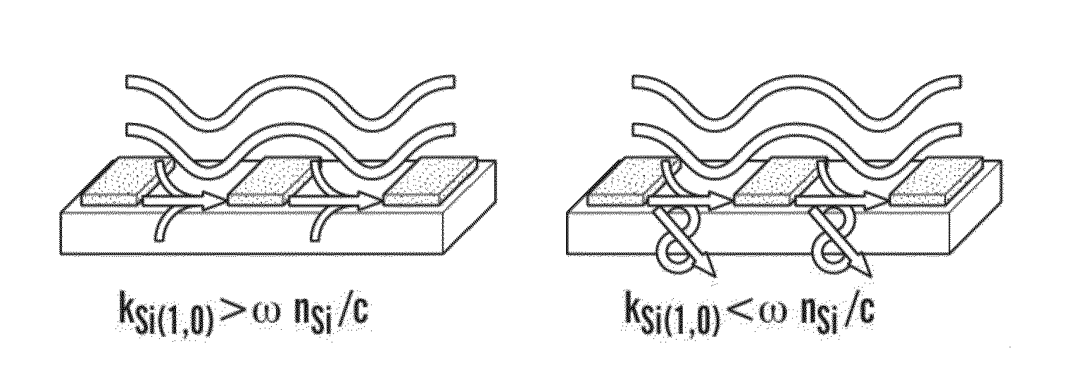
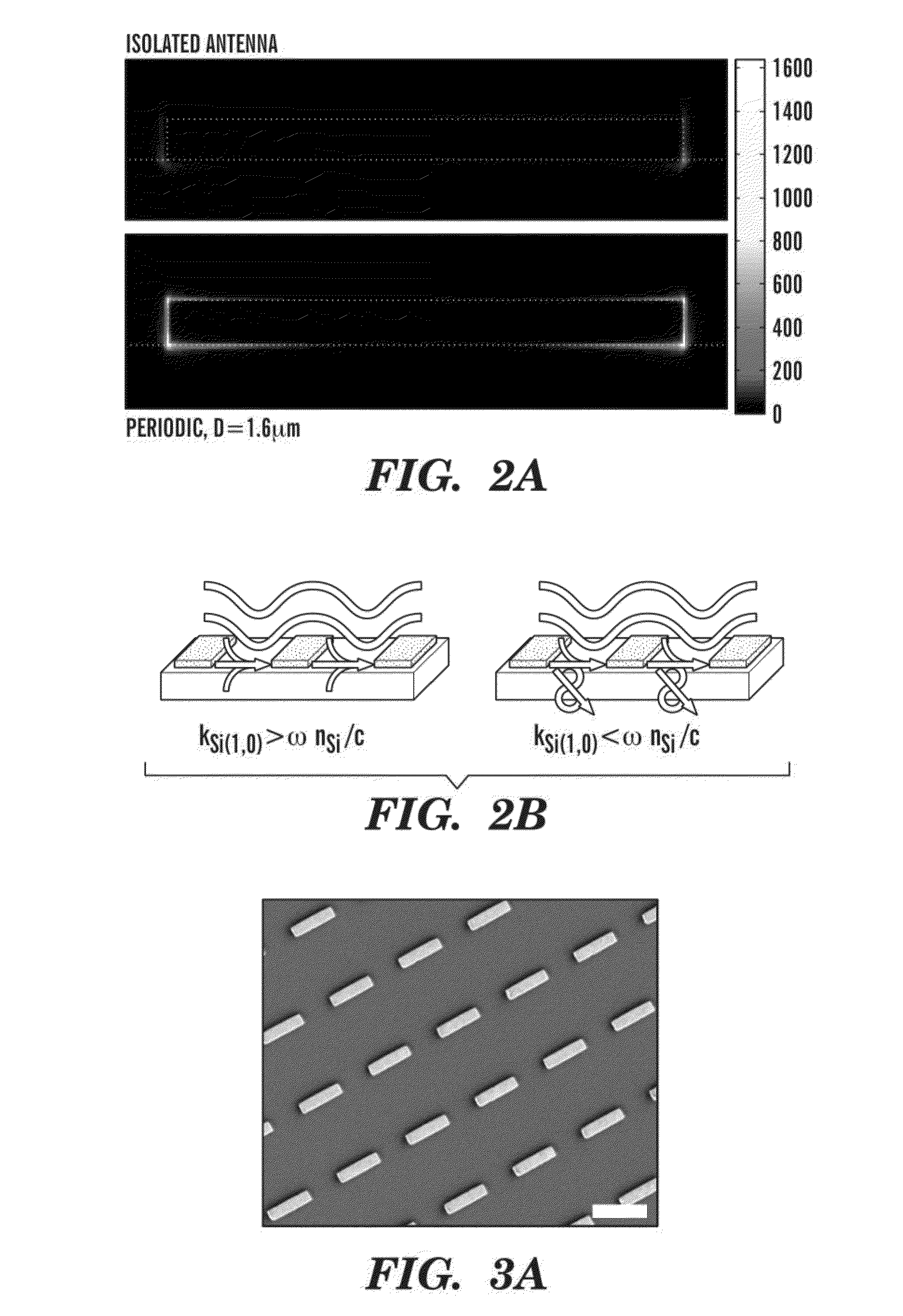
[0276]As disclosed herein, the inventors demonstrate that the engineered nanoantenna arrays can support spectrally well-defined resonances with strong local fields. Furthermore, plasmonic resonances in these nanoantenna arrays can be fine-tuned to specific spectral regions of interest with high spatial reproducibility. Recently, enhanced absorption signals have been observed from individual nanoantennas (Jensen et al., (2000); Applied Spectroscopy 54:371-377., Kundu et al., (2008) Chemical Physics Letters. 452:115-119; Neubrech et al., (2008) Physical Review Letters 101:157403; Bukasov et al., (2009). Analytical Chemistry 81:4531-4535). However, a surprising new phenomena arises as a result of the collective resonant excitation of the spatially and geometrically organized nanoantenna in specific pattern ensembles. In the nanoantenna arrays as disclosed herein, where the nanoantenna (or plasmonic nanostructures) are organized in a predefined pattern on the nanoanten...

example 2

Individual and Collective Resonances of Plasmonic Nanoantennas

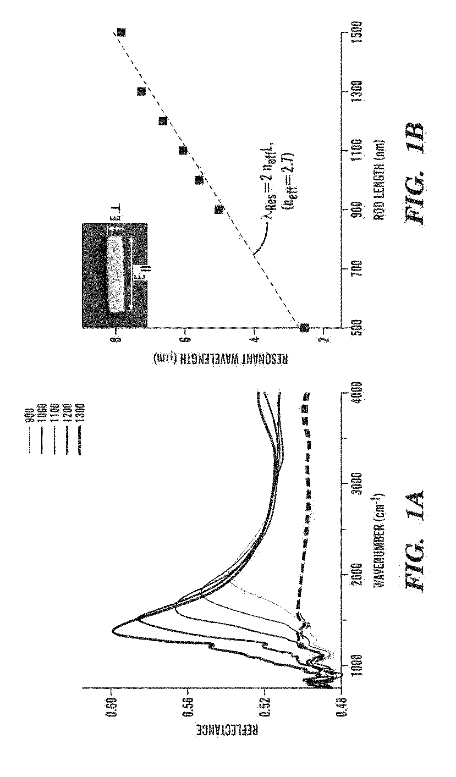
[0284]The plasmonic nanoantenna arrays for enhanced collective response were engineered herein based on the individual antenna behavior. To obtain individual response with a good signal to noise ratio using a conventional Fourier-transform infrared (FTIR) microscope, the nanoantennas were randomly positioned on the support of the array. As previously demonstrated by the inventors, the random arrangement of the nanoantenna array cancels out any diffractive behavior (Yanik et al., (2008) Appl. Phys. Lett. 93:081104). As shown in FIG. 9, the spectral measurements are independent from the randomization process and clearly reflect the individual antenna response. FIG. 1A demonstrates the infrared reflectance measurements from randomized arrays consisting of varying length and a fixed width (230 nm) of nanorods pointing in the same direction on an area of 100×100 μm2. The structures are fabricated on silicon supports using elec...

example 3

SEIRA Enhancement by Collective Resonances

[0288]Direct identification of the vibrational signatures of the protein monolayers is achieved by utilizing this collective excitations. Here, the protein layer is applied to the nanoantenna array surface by uniform spin coating of a thin film of silk fibroin (as described in the material and methods section herein). As mentioned before, a unique advantage of silk is that it allows fine control over the protein film thickness by varying its concentration in solution (Omenetto et al., (2008), Nature Photonics. 2:641-643). Homogeneous films were coated on the nanorod antenna array as thin as 2 nm, corresponding to essentially a single protein monolayer. Atomic force microscopy (AFM) is used to confirm the uniformity and the thickness of the film. Initially, the scanning of the tip is performed in contact mode to scratch away the film down to the silicon support. Subsequent measurements at reduced force are then used to determine the film thic...


PUM


Abstract

The present invention generally relates to nanoantenna arrays and methods of their fabrication. In particular, one aspect relates to nanoantenna arrays comprising nanostructures of predefined shapes in predefined patterns, which results in collective excitement of surface plasmons. In some embodiments the nanoantenna arrays can be used for spectroscopy and nanospectroscopy. Another aspects of the present invention relate to a method of high-throughput fabrication of nanoantenna arrays includes fabricating a reusable nanostencil for nanostensil lithography (NSL) which provides a mask to deposit materials onto virtually any support, such as flexible and thin-film stretchable supports. The nanostencil lithography methods enable high quality, high-throughput fabrication of nanostructures on conducting, non-conducting and magnetic supports. The nanostencil can be prepared by etching nanoapertures of predefined patterns into a waffer or ceramic membrane. In some embodiments, a nanoantenna array comprises plasmonic nanostructures or non-plasmonic nanostructures.

Description

CROSS REFERENCE TO RELATED APPLICATIONS[0001]This application claims priority under 35 U.S.C. 119(e) of U.S. Provisional Patent Application Ser. No. 61 / 279,588 filed on Oct. 23, 2009 and U.S. Provisional Patent Application Ser. No. 61 / 352,654, filed on 8 Jun., 2010 and U.S. Provisional Patent Application Ser. No. 61 / 367,246, filed on 23 Jul., 2010, the contents of which are incorporated herein by reference in their entirety.GOVERNMENT SUPPORT[0002]This invention was made with Government Support under Contract Nos. ECCS-0849603, ECCS-0954790 and EEC-0812056 awarded by the National Science Foundation and Contract No. N0001410-1-0742 awarded by the Office of Naval Research. The Government has certain rights in the invention.FIELD OF THE INVENTION[0003]The present invention is directed to nanoantenna arrays, such as plasmonic nanoantenna arrays and fabrication of nanoantenna arrays. More specifically, the invention provides a nanoantenna arrays comprising plasmonic nanostructures, and m...

Claims


Application Information

Patent Timeline
Patent Type & Authority Applications(United States)
IPC IPC(8): G02B5/00
CPCB82Y15/00B82Y20/00B82Y30/00Y10S977/932G01N21/658G02B5/008G01N21/554
Inventor ALTUG, HATICEYANIK, AHMET ALIERRAMILLI, SHYAMSUNDERADATO, RONENAKSU, SERAPHUANG, MINARTAR, ALP
Owner TRUSTEES OF BOSTON UNIV
Why Eureka
Try Eureka