Selective atomic layer deposition of passivation layers for silicon-based photovoltaic devices

Inactive Publication Date: 2013-06-20
APPLIED MATERIALS INC
View PDF5 Cites 322 Cited by
  • Summary
  • Abstract
  • Description
  • Claims
  • Application Information

AI Technical Summary

Benefits of technology

[0012]In one embodiment, a method includes forming a pattern inhibitor layer on a back surface of a substrate, wherein the pattern inhibitor layer covers a first portion of the back surface and a second portion of the back surface remains substantially free of the pattern inhibitor layer. The method includes forming a passivation layer containing aluminum oxide on the second portion of the back surface while maintaining the pattern inhibitor layer substanti

Problems solved by technology

The efficiency at which a solar cell converts incident light energy into electrical energy is adversely affected by a number of factors.
Each time an electron-hole pair recombines, a charge carrier is eliminated, thereby reducing the efficiency of the solar cell.
Moreover, the efficiency of the solar cell may be reduced due to a reduction in the carrier lifetime caused by a shunt current created at the rear surface of the solar cell.
The excess negative charge can leak into the nearby backside contacts causing recombination to occur at the contact interface, thereby reducing solar cell efficiency.
Shunt current is an undesirable electrical short circuit between the front and back surface contacts of the solar cell.
Patterni

Method used


Image

  • Selective atomic layer deposition of passivation layers for silicon-based photovoltaic devices
  • Selective atomic layer deposition of passivation layers for silicon-based photovoltaic devices
  • Selective atomic layer deposition of passivation layers for silicon-based photovoltaic devices

Examples


Embodiment Construction

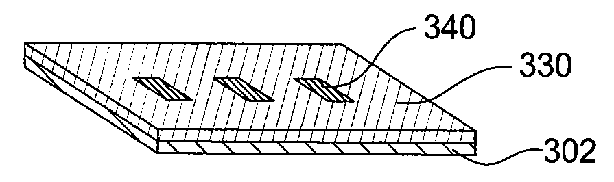
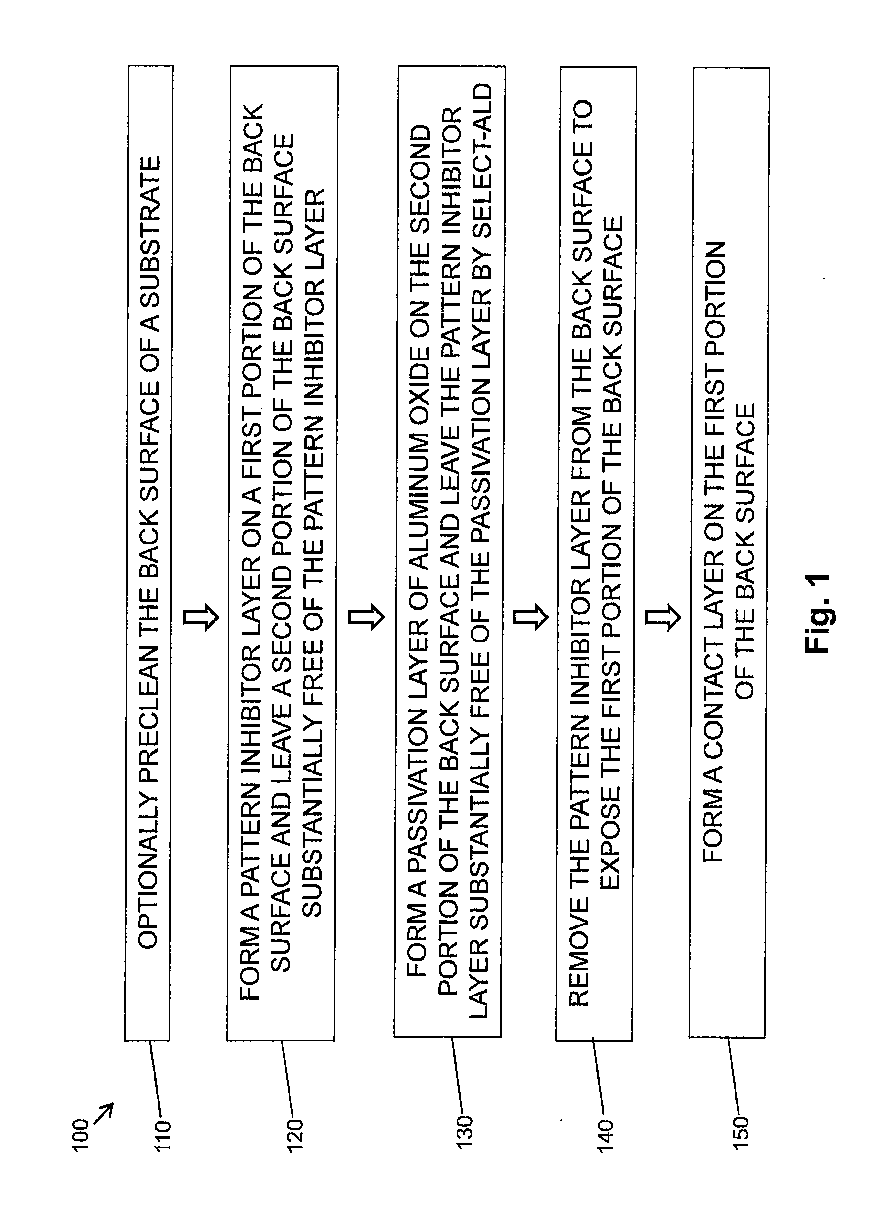
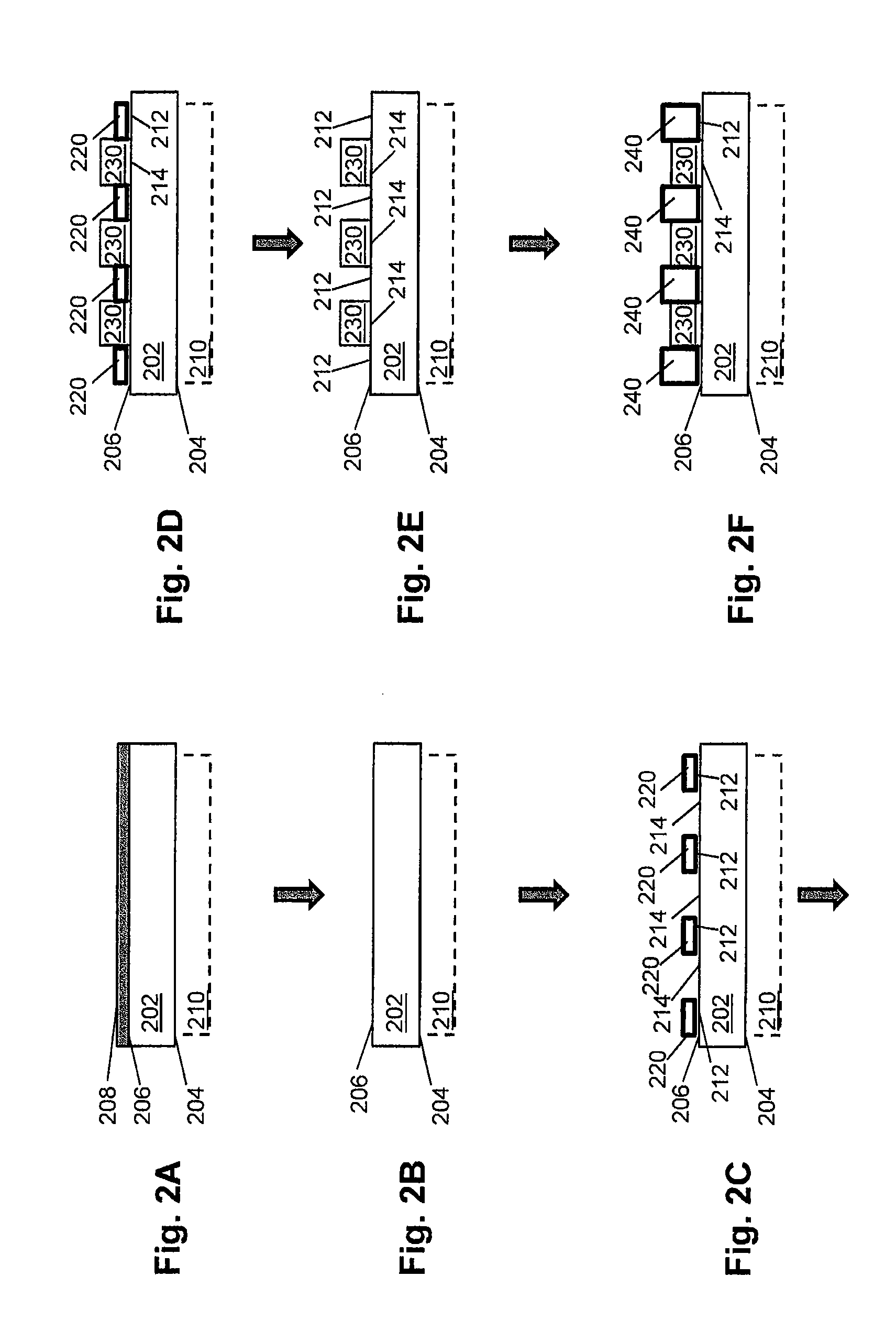
[0024]Embodiments of the invention generally relate to methods for fabricating photovoltaic devices, and more particularly relate to a dielectric passivation and metallization process sequence that includes a selective atomic layer deposition (S-ALD) process utilized to form a passivation layer on the back surface of a silicon-based substrate. The passivation layer is deposited or otherwise formed on selective areas of the back surface of the substrate by the S-ALD process, and subsequently, a metallization contact layer is directly formed on the non-passivated area on the back surface of the substrate. Prior to depositing the passivation layer, a pattern inhibitor layer is printed or otherwise formed on the back surface of the substrate. The pattern inhibitor layer covers a first portion of the back surface and a second portion of the back surface remains substantially free of the pattern inhibitor layer. Thereafter, during the S-ALD process, the passivation layer containing alumin...


PUM


Abstract

Embodiments of the invention generally provide methods for forming a silicon-based photovoltaic device. In one embodiment, a method includes forming a pattern inhibitor layer on a back surface of a substrate, wherein the pattern inhibitor layer covers a first portion of the back surface and a second portion of the back surface remains substantially free of the pattern inhibitor layer. The method further includes forming a passivation layer containing aluminum oxide on the second portion of the back surface and maintaining the pattern inhibitor layer substantially free of the passivation layer during a selective atomic layer deposition (S-ALD) process. Additionally, the method includes removing the pattern inhibitor layer from the back surface to reveal the first portion of the back surface and subsequently forming a contact layer on the first portion of the back surface.

Description

CROSS-REFERENCE TO RELATED APPLICATIONS[0001]This application claims benefit of U.S. provisional patent application No. 61 / 576,864, filed Dec. 16, 2011, which is hereby incorporated by reference.BACKGROUND OF THE INVENTION[0002]1. Field of the Invention[0003]Embodiments of the invention generally relate to methods for fabricating photovoltaic devices, and more particularly to methods for selective atomic layer deposition of passivation layers on the back surfaces of silicon-based solar substrates.[0004]2. Description of the Related Art[0005]Solar cells are photovoltaic devices that convert sunlight directly into electrical power. The most common material utilized in a solar cell is silicon, which is generally in the form of single crystalline silicon, polycrystalline silicon, or amorphous silicon. The ratio of light converted into electrical power versus the amount of light shined on the front or light-receiving surface of the solar cell is a measurement of the efficiency of the sol...

Claims


Application Information

Patent Timeline
IPC IPC(8): H01L31/18
CPCH01L31/18H01L21/76802Y02E10/50H01L31/02167
Inventor VAIDYA, KAUSHIKPONNEKANTI, HARI K.
Owner APPLIED MATERIALS INC
Why Eureka
Try Eureka