

POLYCRYSTALLINE ALUMINUM NITRIDE BASE MATERIAL FOR CRYSTAL GROWTH OF GaN-BASE SEMICONDUCTOR AND METHOD FOR MANUFACTURING GaN-BASE SEMICONDUCTOR USING THE SAME
a technology of gan-base semiconductor and polycrystalline aluminum nitride, which is applied in the direction of basic electric elements, chemical vapor deposition coating, coating, etc., can solve the problems of high cost (sapphire and sic), difficulty in increasing the size of the substrate, etc., and achieve good yield
- Summary
- Abstract
- Description
- Claims
- Application Information
AI Technical Summary
Benefits of technology
Problems solved by technology
Method used
Image

Examples
examples 6 to 10
[0061]An aluminum nitride powder (mean particle diameter 0.8 μm, oxygen content 1.0% by weight) (97% by weight) and 3% by weight of a yttria (Y2O3) powder (mean particle diameter 1.2 μm) were mixed together to prepare a starting material powder.
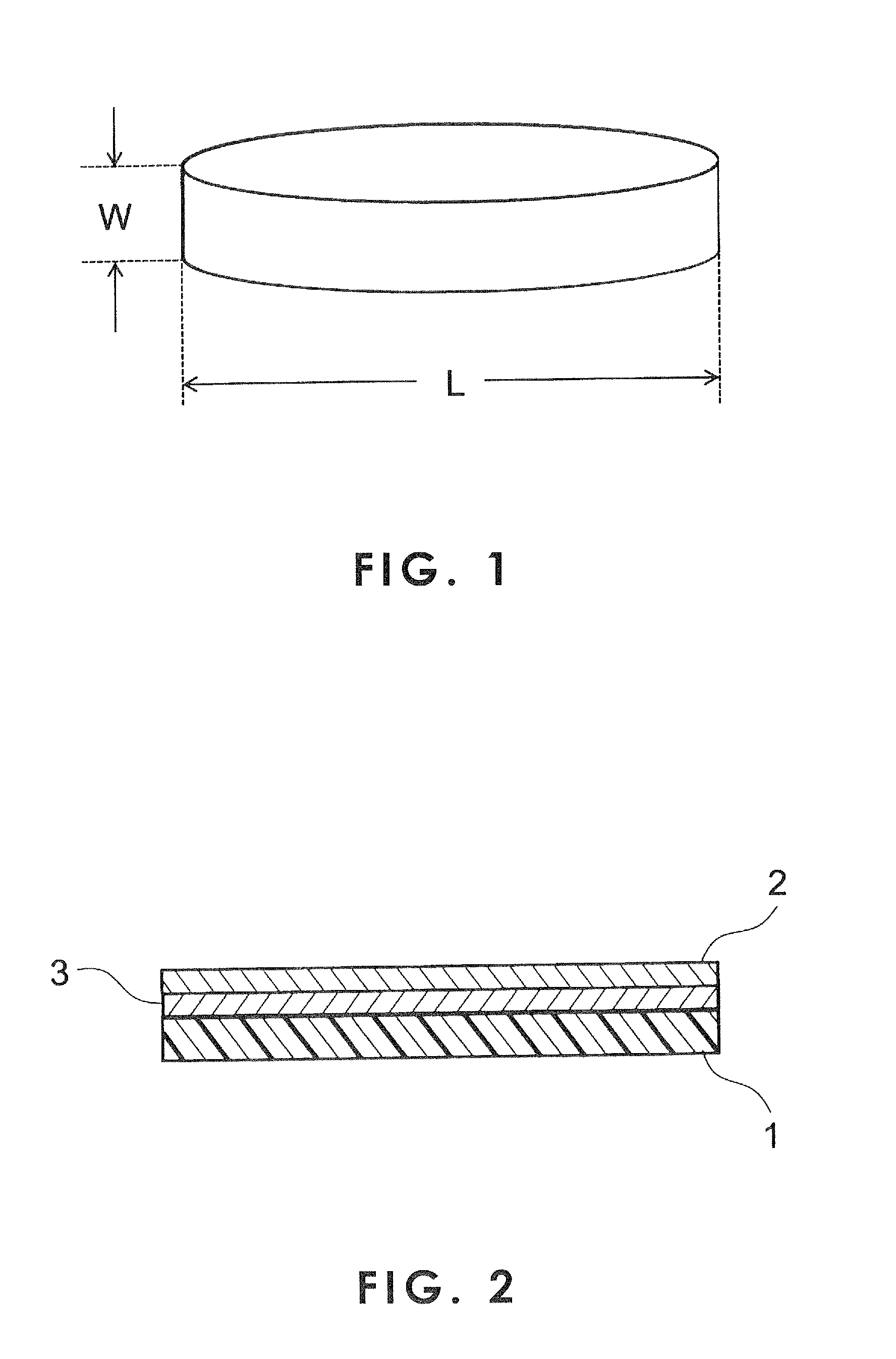
[0062]In the mixing, the starting material powder was added to a solvent such as toluene or ethanol, and an organic binder and a plasticizer were further added thereto, followed by mixing to prepare a starting material slurry. A green sheet having a thickness of 1.2 mm was formed by doctor blading using the starting material slurry thus obtained. The green sheet was cut into pieces having a size of 170 mm in length×170 mm in width that were then degreased, was sintered at 1700° C. to 1850° C. for 3 hr to 5 hr in a nitrogen atmosphere pressurized to 2 kPa to obtain a polycrystalline aluminum nitride substrate. The polycrystalline aluminum nitride substrate thus obtained was subjected to a first polishing step with a diamond wheel of #300 and a...
examples 6a to 10a
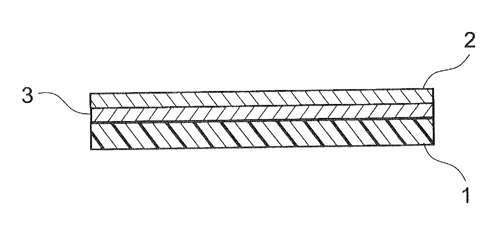
[0071]The polycrystalline aluminum nitride substrates of Examples 6 to 10 were fabricated into a disk having a size of 6 inches (152.4 mm) in diameter×1 mm in thickness and a surface roughness (Ra) of 0.01 μm. Crystals of GaN semiconductors were grown using the samples.
[0072]The sample (polycrystalline aluminum nitride substrate) was placed on a susceptor within a MOCVD device. A GaN buffer layer was formed by a metal-organics chemical vapor deposition method (MOCVD method) at 500° C. to 600° C. while allowing a TMG gas (trimethyl gallium gas) and an ammonium gas to flow. The thickness of the GaN layer was increased (by crystal growth) at 1000° C. to 1100° C. The thickness of the buffer layer was 0.02 μm, and the final thickness of the GaN layer was 3 μm. The GaN layer was provided on the surface of the polycrystalline aluminum nitride substrate (diameter 6 inches).
[0073]The presence or absence of layer separation was determined for the GaN-base semiconductors thus obtained in the s...
PUM
| Property | Measurement | Unit |
|---|---|---|
| diameter | aaaaa | aaaaa |
| thermal conductivity | aaaaa | aaaaa |
| diameter | aaaaa | aaaaa |
Abstract
Description
Claims
Application Information