Photoelectric conversion material, film containing the material, photoelectric conversion device, method for preparing photoelectric conversion device, method for using photoelectric conversion device, photosensor and imaging device

a technology of photoelectric conversion and conversion device, which is applied in thermoelectric devices, triarylamine dyes, methine/polymethine dyes, etc., can solve the problems of low light utilization efficiency, small photodiode parts, and insufficient light transmission through color filters. , to achieve the effect of high charge collection efficiency, low dark current property, and high speed response property

Active Publication Date: 2013-07-18
FUJIFILM CORP
View PDF2 Cites 35 Cited by
  • Summary
  • Abstract
  • Description
  • Claims
  • Application Information

AI Technical Summary

Benefits of technology

[0105]According to the present invention, a film can be formed by deposition at a high temperature without causing materials to be decomposed, and thus, it is possible to provide a compound capable of providing a photoelectric conversion device having high charge collection efficiency, high speed res

Problems solved by technology

In this single-plate solid-state imaging device, since the color filter transmits only light at a limited wavelength, light not transmitted through the color filter is not utilized and the light utilization efficiency tends to be low.
As a result, the area of a photodiode part becomes smaller and problems such as the reduction in the aperture ratio and the reduction in the light collection efficiency arise.
However, in these methods, there are disadvantages in that the color separation is insufficient because the absorption range in each light receiving unit has an overlapped portion in the depth direction of Si, and thus, spectral characteristics are poor.
In the case of making the photoelectric conversion efficiency high by the introduction of a p-n junction or a bulk hetero-structure, increase in dark current

Method used


Image

  • Photoelectric conversion material, film containing the material, photoelectric conversion device, method for preparing photoelectric conversion device, method for using photoelectric conversion device, photosensor and imaging device
  • Photoelectric conversion material, film containing the material, photoelectric conversion device, method for preparing photoelectric conversion device, method for using photoelectric conversion device, photosensor and imaging device
  • Photoelectric conversion material, film containing the material, photoelectric conversion device, method for preparing photoelectric conversion device, method for using photoelectric conversion device, photosensor and imaging device

Examples


example 1-1

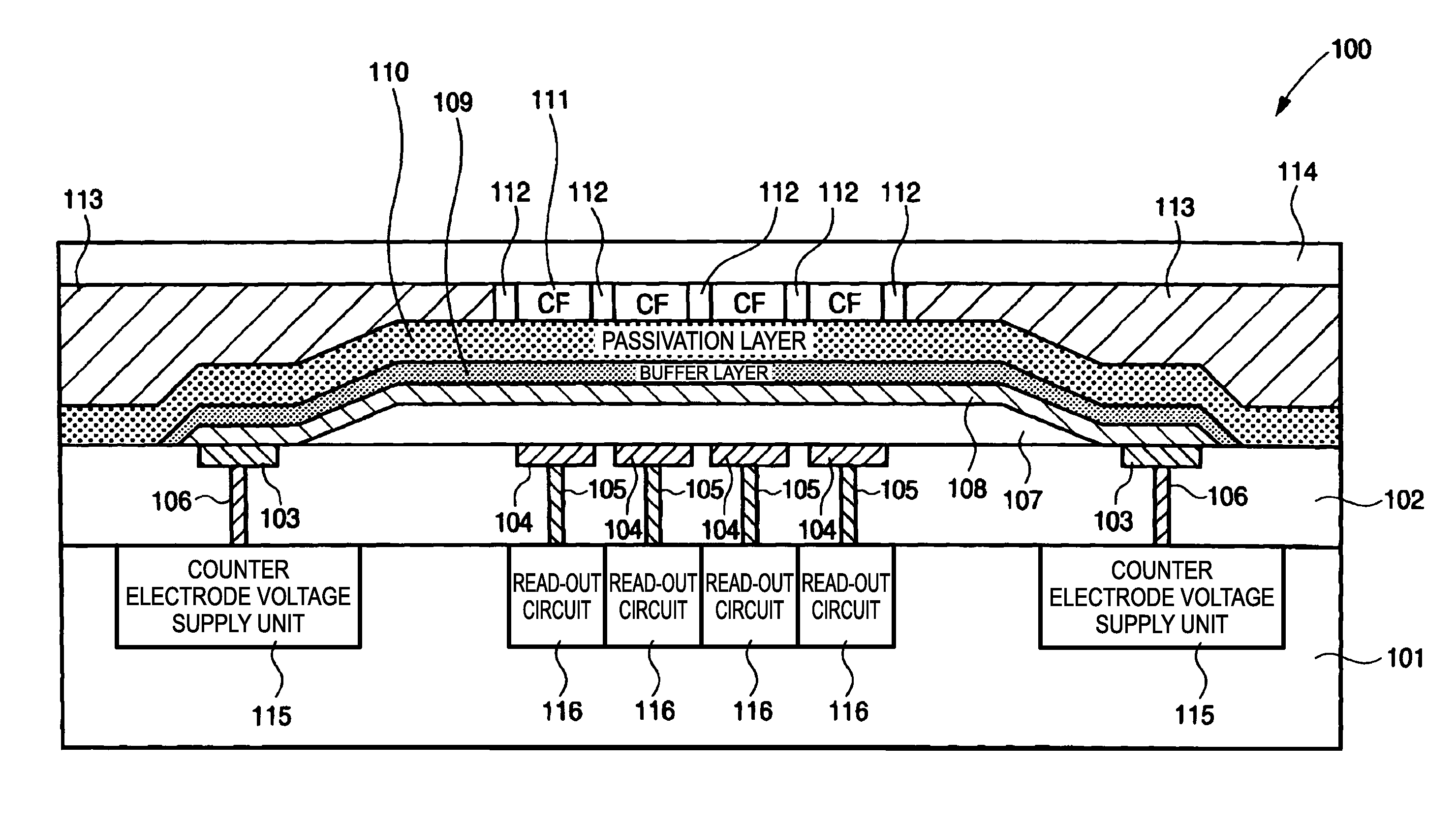
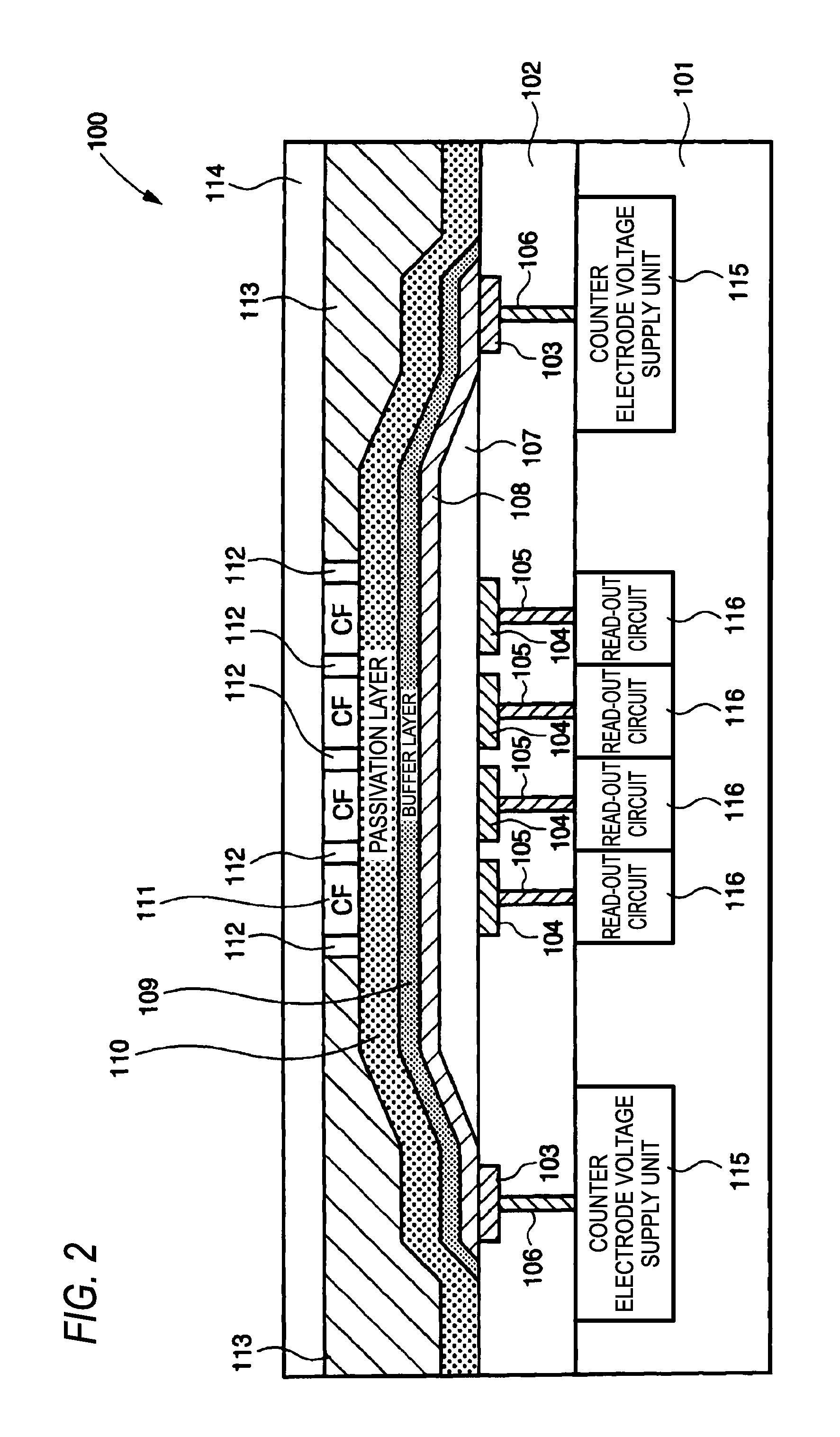
[0459]A solid-state imaging device including a photoelectric conversion device having a configuration as, illustrated in FIG. 2 was fabricated. Here, the photoelectric conversion device was constituted with a lower electrode (104), a photoelectric conversion film (107) and an upper electrode (108), and an organic photoelectric conversion film including a photoelectric conversion layer and an electron blocking layer was formed as the photoelectric conversion film (107). That is, amorphous ITO of 30 nm was formed on a glass substrate by a sputtering method to fabricate a lower electrode. Compound (B-1) of 100 nm was formed by a vacuum heating deposition method to form an electron blocking layer. Further, thereon, a layer, which was formed by co-depositing Compound (A-1) and fullerene (C60) so as to be 100 nm and 300 nm, respectively, in terms of a single layer, was formed by a vacuum heating deposition in a state where the temperature of the substrate was controlled to 25° C. to form ...

examples 1-2 to 1-26

and Comparative Examples 1-1 to 1-6

[0460]Photoelectric conversion devices were fabricated in the same manner as in Example 1-1, except that, and compounds (B-1) and (A-1) used in the electron blocking layer and the photoelectric conversion material were changed as shown in Table 2.

[Evaluation]

[0461]Each of the devices obtained was checked whether it functions as a photoelectric conversion device. It is confirmed that, when voltage is applied to the lower electrode and the upper electrode of each of the devices obtained so as to be an electric field strength of 2.5×10⁵ V / cm, any devices show a dark current of 100 nA / cm2 or less in a dark place, but show a current of 10 μA / cm2 or more in a bright place, thereby functioning as a photoelectric conversion device.

[0462]The relative response speed (a vertical rise time with a signal strength of from 0% to 90%) (a relative value when the 1st batch in Example 1-1 is counted as 1) when an electric filed of 2×10⁵ V / cm was applied to the photoe...

example 2-1

[0467]A solid-state imaging device including a photoelectric conversion device having a configuration as illustrated in FIG. 2 was fabricated. Here, the photoelectric conversion device was constituted with a lower electrode (104), a photoelectric conversion film (107) and an upper electrode (108), and an organic photoelectric conversion film including a photoelectric conversion layer and an electron blocking layer was formed as the photoelectric conversion film (107). That is, amorphous ITO of 30 nm was formed on a glass substrate by a sputtering method to fabricate a lower electrode. Compound (B-1) of 100 nm was formed by a vacuum heating deposition method to form an electron blocking layer. Further, thereon, a layer, which was formed by co-depositing Compound (A-1) and fullerene (C60) so as to be 100 nm and 300 nm, respectively, in terms of a single layer, was formed by a vacuum heating deposition in a state where the temperature of the substrate was controlled to 25° C. to form a...


PUM

PropertyMeasurementUnit
Temperatureaaaaaaaaaa
Nanoscale particle sizeaaaaaaaaaa

Abstract

There is provided a compound represented by a specific formula, which has an absorption maximum at 400 nm or more and less than 720 nm in a UV-visible absorption spectrum, wherein a molar extinction coefficient is 10,000 mol−1·l·cm−1 or more at the absorption maximum wavelength, and a difference between a melting point and a deposition temperature (a melting point−a deposition temperature) is 31° C. or more.

Description

TECHNICAL FIELD[0001]The present invention relates to a compound useful for a photoelectric conversion device material, a photoelectric conversion material, a film containing the material, photoelectric conversion device, a method for preparing a photoelectric conversion device, a method for using a photoelectric conversion device, a photosensor and an imaging device.BACKGROUND ART[0002]As a conventional photosensor, a device fabricated by forming a photodiode (PD) on a semiconductor substrate such as silicon (Si) is general. As for a solid-state imaging device, a flat solid-state imaging device is widely used, in which PDs are two-dimensionally arranged in a semiconductor substrate and a signal according to a signal charge generated by photoelectric conversion in each PD is read out through a CCD or CMOS circuit.[0003]As a method for achieving a color solid-state imaging device, a structure in which a color filter transmitting only light at a specific wavelength for a color separat...

Claims


Application Information

Patent Timeline
IPC IPC(8): H01L51/00
CPCC07D219/02Y02E10/549C07D455/03C07D455/06C07D471/14C07D471/16H01L51/0052H01L51/0059H01L51/0072H01L51/0094H01L51/4206H01L51/4273H01L51/0058C07C225/22C07D221/18C09B21/00C09B23/04C09B57/008H10K85/615H10K85/631H10K85/626H10K85/40H10K85/6572H10K30/451H10K30/353
Inventor YOFU, KATSUYUKINOMURA, KIMIATSUFUKUZAKI, EIJIHIRAI, YUKIHAMANO, MITSUMASAMITSUI, TETSURO
Owner FUJIFILM CORP
Why Eureka
Try Eureka