Method for producing graphene at a low temperature, method for direct transfer of graphene using same, and graphene sheet
a graphene sheet and low temperature technology, applied in the direction of non-metal conductors, plasma techniques, conductors, etc., can solve the problems of increasing cost, unable to meet the expectations of electrical and mechanical characteristics, and limited research on practically applicable technologies, etc., to achieve convenient production, large area, and high production efficiency
- Summary
- Abstract
- Description
- Claims
- Application Information
AI Technical Summary
Benefits of technology
Problems solved by technology
Method used
Image
Examples
example 1
Low-Temperature Growth and Transfer of Graphene Onto Polyimide (PI) Polymer Sheet Substrate
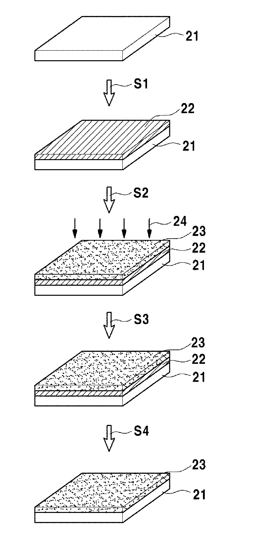
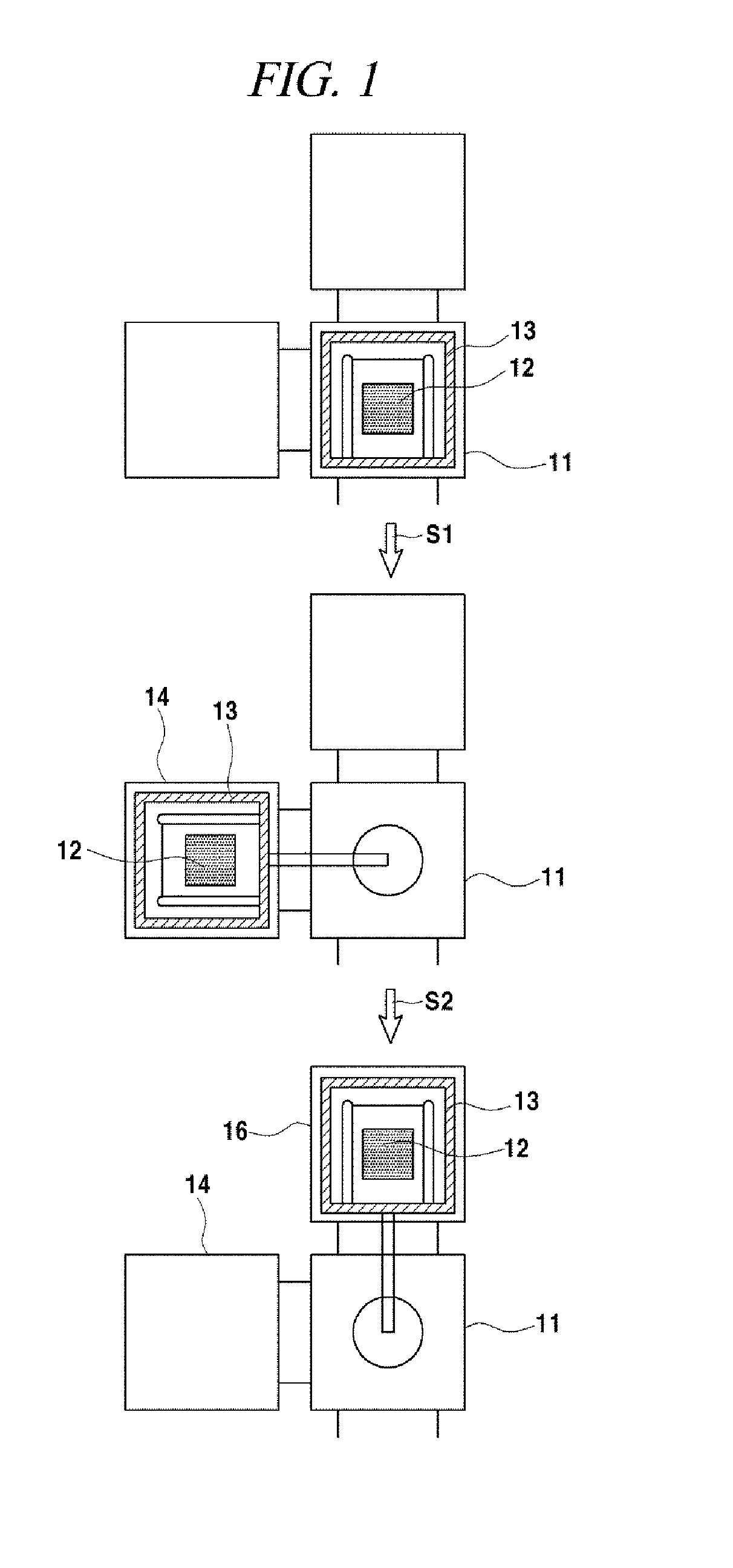
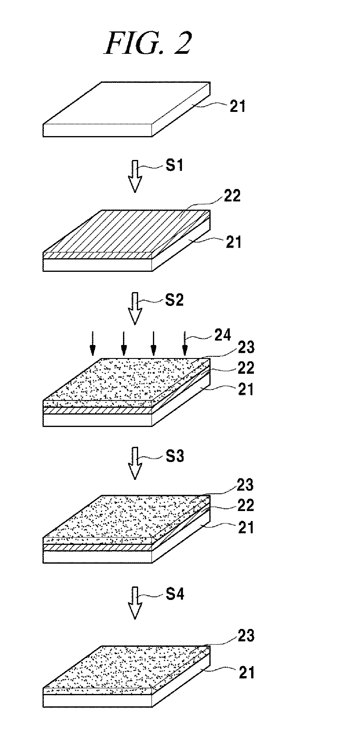
[0103]Graphene was produced and directly transferred onto a polyimide (PI) polymer sheet substrate by using an apparatus illustrated in FIG. 1 through a process illustrated in FIG. 2. To be specific, the polyimide (PI) polymer sheet substrate was loaded into a deposition chamber by using a load-locked chamber and a Ni layer and a Cu layer patterned in various ways as metal catalyst layers for growing graphene were respectively deposited with a thickness of about 150 nm by a RF sputtering method. Then, the substrate on which the catalyst layers were deposited was unloaded from the deposition chamber to the load-locked chamber and loaded into an ICP-CVD chamber. The substrate was annealed at a temperature of about 300° C. with a hydrogen gas. Thereafter, a carbon and argon-containing gas (C2H2: Ar=60:2 sccm) was supplied thereto at about 20 mTorr for about 15 seconds to about 3 minutes to produc...
example 2
Low-Temperature Growth and Transfer of Graphene Onto Aluminum Foil Substrate
[0111]By using an apparatus illustrated in FIG. 1 and commercial aluminum foil as a substrate, a graphene sheet was grown at a low temperature and produced on the aluminum foil. To be specific, the aluminum foil substrate was loaded into an ICP-CVD chamber by using a load-locked chamber and annealed at a temperature of from about 300° C. to about 500° C. with a hydrogen gas. Thereafter, a carbon and argon-containing gas (C2H2:Ar=60:2 to 1 sccm) was supplied thereto at about 20 mTorr for about 15 seconds to about 3 minutes to produce graphene on the aluminum (Al) layer by means of ICP-CVD. Then, the graphene was cooled at a speed of about 5° C. / s at room temperature within the ICP-CVD chamber, so that a graphene sheet grown on the Al layer was obtained. Thereafter, the Al layer was etched and removed by using a FeCl3 solution and the separated and floated graphene sheet was transferred onto a silicon wafer. A...
example 3
[0112]Low-Temperature Growth and Transfer of Graphene Onto Zinc Substrate
[0113]By using an apparatus illustrated in FIG. 1 and commercial zinc substrate as a substrate, a graphene sheet was grown at a low temperature and produced on the zinc substrate. To be specific, the zinc substrate was loaded into an ICP-CVD chamber by using a load-locked chamber and annealed at a temperature of from about 300° C. to about 500° C. with a hydrogen gas. Thereafter, a carbon and argon-containing gas (C2H2:Ar=60:3 to 5 sccm) was supplied thereto at about 20 mTorr for about 5 minutes to about 10 minutes to produce graphene on the zinc (Zn) layer by means of ICP-CVD. Then, the graphene was cooled at a speed of about 5° C. / s at room temperature within the ICP-CVD chamber, so that a graphene sheet grown on the Zn layer was obtained. A photograph and a Raman spectrum graph of a graphene sheet grown on the Zn substrate illustrated in FIGS. 15 and 16, respectively. In the Raman spectrum of FIG. 16, Al 1 a...
PUM
| Property | Measurement | Unit |
|---|---|---|
| temperature | aaaaa | aaaaa |
| sheet resistance | aaaaa | aaaaa |
| transparency | aaaaa | aaaaa |
Abstract
Description
Claims
Application Information


