

Conductive paste for use in photovoltaic cell and method of producing photovoltaic cell element using the same
a photovoltaic cell and conductive paste technology, applied in the direction of non-conductive materials with dispersed conductive materials, conductors, metal/alloy conductors, etc., can solve the problems of poor contact between the semiconductor substrate and the electrode, the surface cracking of the semiconductor substrate tends to occur, and the electrode tends to peel away, so as to reduce the failure rate, reduce the occurrence of cracking, and reduce the effect of poor conta
- Summary
- Abstract
- Description
- Claims
- Application Information
AI Technical Summary
Benefits of technology
Problems solved by technology
Method used
Image

Examples
example 1
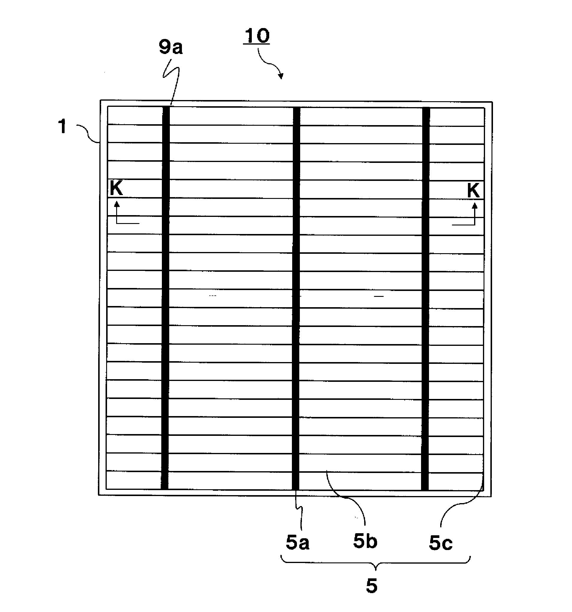
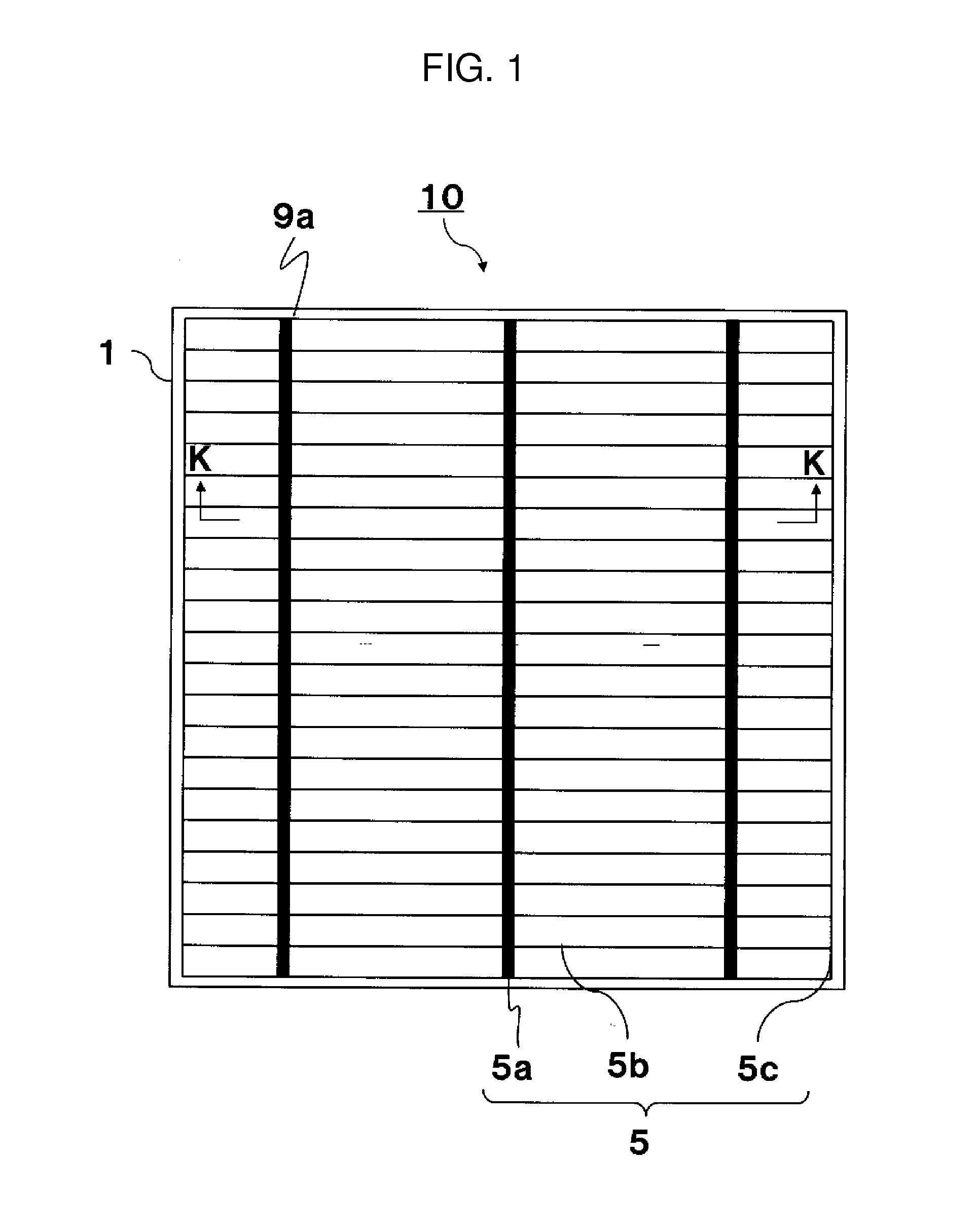
[0066]First, a polycrystalline silicon substrate (the semiconductor substrate 1) having a thickness of 260 μm, an outer shape of 156 mm×156 mm, and a resistivity of 1.5 Ω-cm were prepared and the damaged layer at the surface of the silicon substrate was etched by an NaOH solution and washed.
[0067]Next, dry etching was used to form a texture on the first surface 9a. Then, vapor-phase thermal diffusion method, in which POCl3 is used as a source in the diffusion process, was used to form the second semiconductor layer 3. When this was done, the sheet resistance of the second semiconductor layer 3 was 70 Ω / square. A hydrofluoric acid solution was used to remove phosphorus glass by etching, p-n separation was performed by a laser beam, and then a silicon nitride film to serve as the anti-reflection layer 4 was formed on the first surface 9a using PECVD.
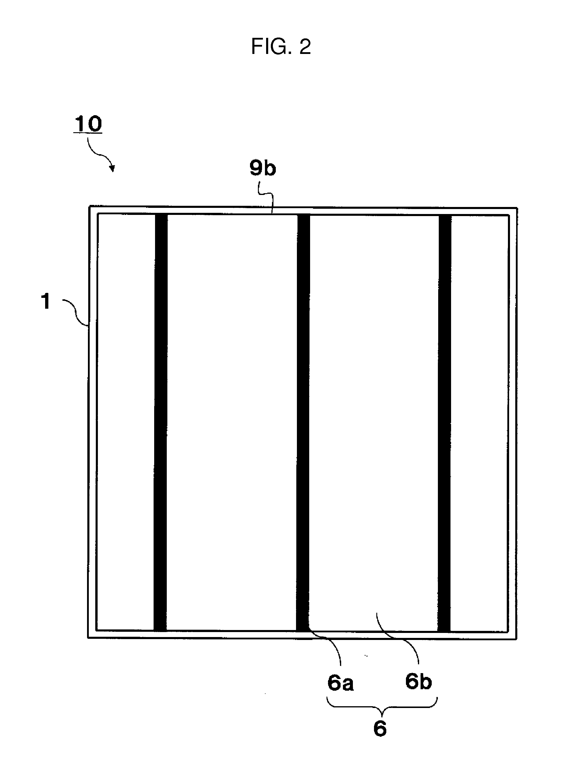
[0068]Additionally, an aluminum paste was coated over the substantially entire surface of the second surface 9b of the semiconductor subs...
example 2
[0076]Next, whereas a Bi2O3 based glass was used as a glass frit in the paste to be used for the first electrode 5, a photovoltaic cell element using a paste to which the prescribed sintering inhibitor was added will be described as an example.
[0077]Because it was the same as the example 1, except mainly for the materials of the glass frit in the above-noted pastes and the formation by using only the above-noted paste without providing the silver plated electrode layer in the first electrode 5, the detailed description will be omitted.
[0078]Two kinds of glass frits that substantially included and did not include B2O3 in the glass were prepared.
[0079]In the glass frit B that substantially included B2O3 in the glass, the included mass amounts, with respect to the overall glass frit taken as 100 mass %, was 75 mass % of Bi2O3, 2 mass % of SiO2, 11 mass % of ZnO, and 9 mass % of B2O3, with other components (ZrO2, BaO, MgO, CaO, TiO2, Cr2O3, Fe2O3, Al2O3, CuO and / or P2O5 or the like) bei...
example 3
[0087]Next, a photovoltaic cell element 10 having the first electrode 5 that was formed using a paste that included the glass frit A and a photovoltaic cell element 10 having the first electrode 5 that was formed using a paste that included the glass frit C were fabricated.
[0088]Because it was the same as the example 1, except mainly for the materials of the glass frit in the above-noted pastes and the formation by using only the above-noted paste without providing the silver plated electrode layer in the first electrode 5, the detailed description will be omitted.
[0089]The included mass amount of the glass frit with respect to the included mass amount of a silver powder in the paste was 5%, and Al2O3 was used as the sintering inhibitor composition. In Table 4, the sintering inhibitor indicates the mass % of the sintering inhibitor with respect to the total included mass amount of silver powder and the glass frit.
[0090]An interconnect member made of the copper foil was connected to ...
PUM
| Property | Measurement | Unit |
|---|---|---|
| thickness | aaaaa | aaaaa |
| diameter | aaaaa | aaaaa |
| particle diameter | aaaaa | aaaaa |
Abstract
Description
Claims
Application Information