

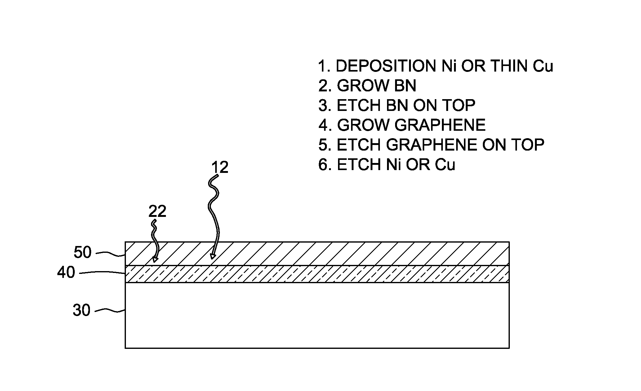
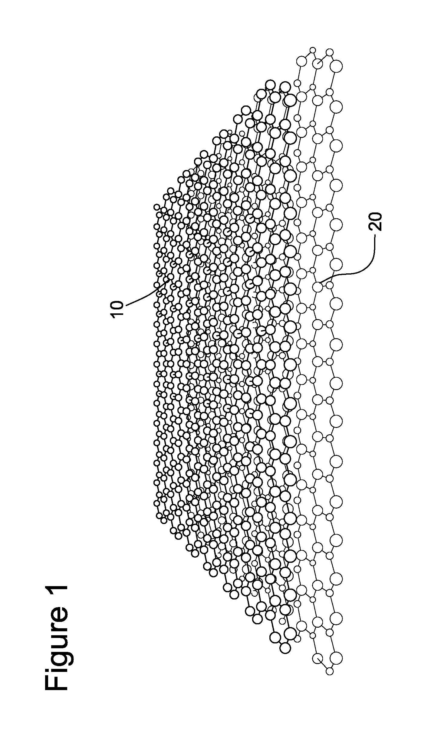
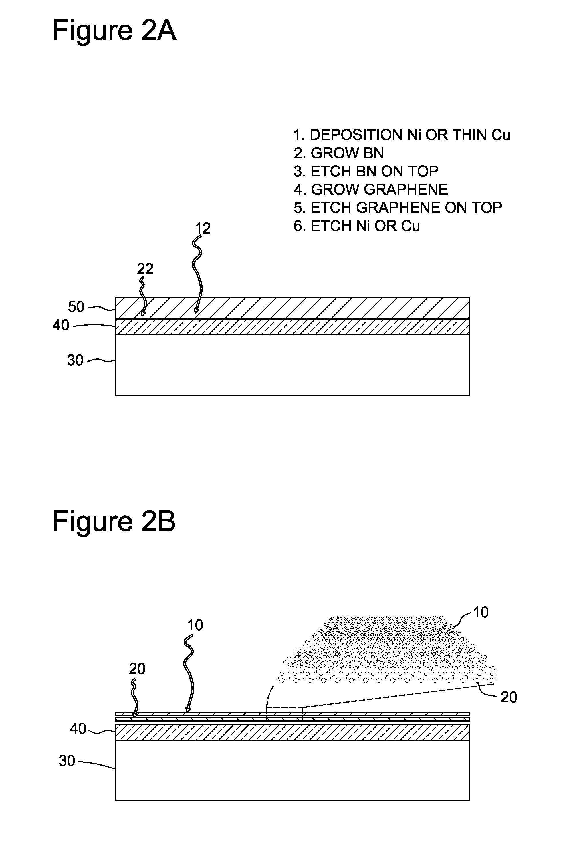
Direct and sequential formation of monolayers of boron nitride and graphene on substrates
a technology of boron nitride and graphene, which is applied in the direction of material nanotechnology, semiconductor devices, electrical apparatus, etc., can solve the problems of difficult atomic thickness of sheets, low yield and a significant density of folds and tears, and the transfer process of graphene from a metal (a) is not feasible for large-scale synthesis
- Summary
- Abstract
- Description
- Claims
- Application Information
AI Technical Summary
Benefits of technology
Problems solved by technology
Method used
Image

Examples
example 1
Direct Growth of Graphene on Silicon Oxide on Silicon
[0062]An approximately 5 centimeter (two inch) diameter silicon dioxide layer having a thickness of 90 nanometers was formed on an n-type (n++) silicon substrate. The substrate was cleaned by using oxygen plasma (100 W, 600 mTorr, 2 min). A layer of PMMA was spin-coated (1% in acetone, 4000 rpm (as an example)) on the silica substrate to a thickness of about 10 nm. A 400 nm thick nickel layer was deposited on the PMMA layer in a metal evaporator system. The metal-on-PMMA-on-silica-on-silicon substrate was put inside a CVD chamber. The sample was baked at 1000° C. for 5 min to anneal the film. The atmosphere comprised hydrogen gas at a pressure of 7 Torr. Finally, the sample was rapidly cooled at 10° C. / second to room temperature. This produced graphene at the interface between metal and silica. Finally, the metal film was etched with iron (III) nitrate, rendering graphene on silica-on-silicon substrate.
example 2
Direct Growth of Graphene on Silicon Oxide on Silicon
[0063]An approximately 5 centimeter (two inch) diameter silicon dioxide layer having a thickness of 90 nanometers was formed on an n-type (n++) silicon substrate. The substrate was cleaned by using oxygen plasma (100 W, 600 mTorr, 2 min). A 400 nm thick nickel layer was deposited on the silicon dioxide layer in a metal evaporator system. The metal-on-silica-on-silicon substrate was put inside a CVD chamber. The sample was baked at 1000° C. for 5 min to anneal the film. The atmosphere comprised methane and hydrogen gas in a molar ration of 1:10 methane:hydrogen at a pressure of 100 Torn Finally, the sample was rapidly cooled at 10° C. / second to room temperature. This produced graphene at the interface between metal and silica. Finally, the metal film was etched with iron (III) nitrate, rendering graphene on silica-on-silicon substrate.
example 3
Direct Growth of Graphene on BN-SiO2-on-Silicon
[0064]An approximately 5 centimeter (two inch) diameter silicon dioxide layer having a thickness of 300 nanometers was formed on an n-type (n++) silicon substrate. The substrate was cleaned by using oxygen plasma (100 W, 600 mTorr, 2 min). Hexagonal boron nitride (hBN) flake / sheet were mechanically exfoliated and transferred onto 300 nm SiO2 substrate via Scotch tape's method and washed. Subsequently, the substrate was sputtered with thin film of copper (100 nm-300 nm) using cold sputtering system. CVD growth was performed under atmosphere pressure in 4″quartz tube with the total gas flow of 100 sccm of hydrogen gas (5-10 sccm) and methane gas (95-90 sccm) at 1000° C. for 40 min. Finally, the top graphene film was O2 plasma-etched and copper is washed. Raman spectroscopy revealed the signature boron nitride and G-peak of graphene.
PUM
 Abstract
Description
Claims
Application Information