
Non-polar plane of wurtzite structure material

a technology of wurtzite and epitaxy layer, which is applied in the direction of polycrystalline material growth, crystal growth process, chemically reactive gas, etc., can solve the problems of reducing the light-emitting quantum efficiency, achieve improved optical properties, maintain thermal stability, and reduce mismatch between substrate and epitaxial layer.

Active Publication Date: 2013-09-19
NAT CHIAO TUNG UNIV
View PDF3 Cites 8 Cited by
  • Summary
  • Abstract
  • Description
  • Claims
  • Application Information

AI Technical Summary

Benefits of technology

The present invention provides a method for growing a non-polar (13 (40)) plane epitaxy layer of wurtzite structure using a single crystal oxide as a substrate. The non-polar crystal plane is grown on a specific cross section of the substrate, resulting in improved optical properties, reduced mismatch between the substrate and epitaxial layer, and better optical properties than existing non-polar a-plane and m-plane. The invention also provides a non-polar (13 (40)) plane epitaxy layer that prevents the offsets of valence band and conduction band caused by the polarization effect, and a photoelectric device using the non-polar (13 (40)) plane epitaxy layer as a semiconductor material. The invention improves the light emitting efficiency of optical elements through eliminating polarity and has a great prospect for applications in light emitting devices.

Problems solved by technology

Prior studies show that GaN grown in the direction along c axis may present a planar arrangement and induce a built-in electric field by polarization effect, which in turn, results in the offsets of valence band and conduction band, thus reducing the light-emitting quantum efficiency.

Method used


Image

  • Non-polar plane of wurtzite structure material
  • Non-polar plane of wurtzite structure material
  • Non-polar plane of wurtzite structure material

Examples


example 1

Growth of the Non-Polar (13 40) Crystal Plane Of Oxide Zinc

[0031]First, a single crystal oxide with perovskite structure was provided, wherein the single crystal oxide was a 2-inch LaAlO3 (LAO) single crystal oxide with a thickness of 0.5 nm.

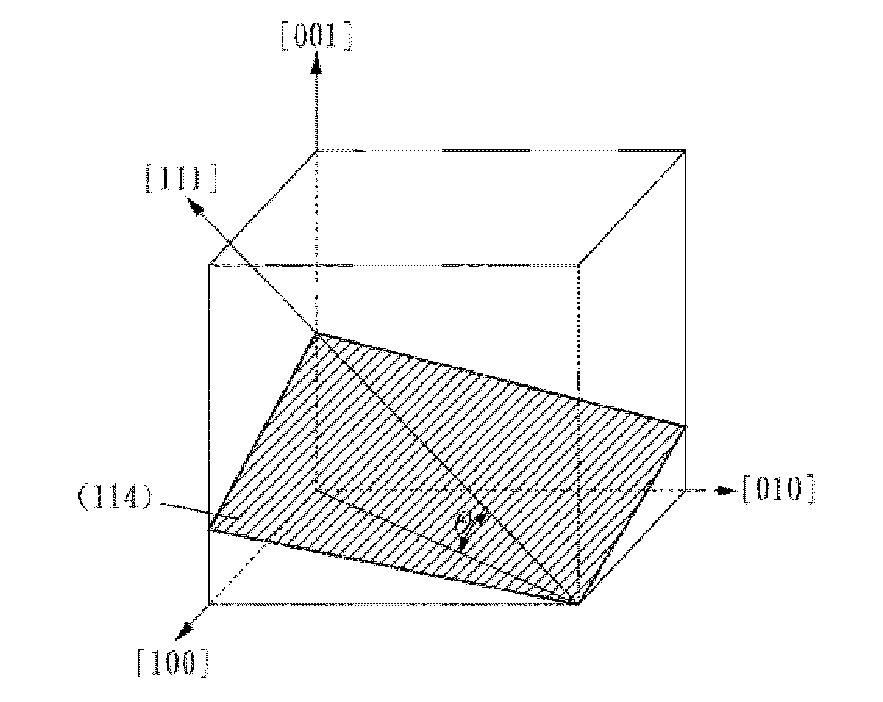
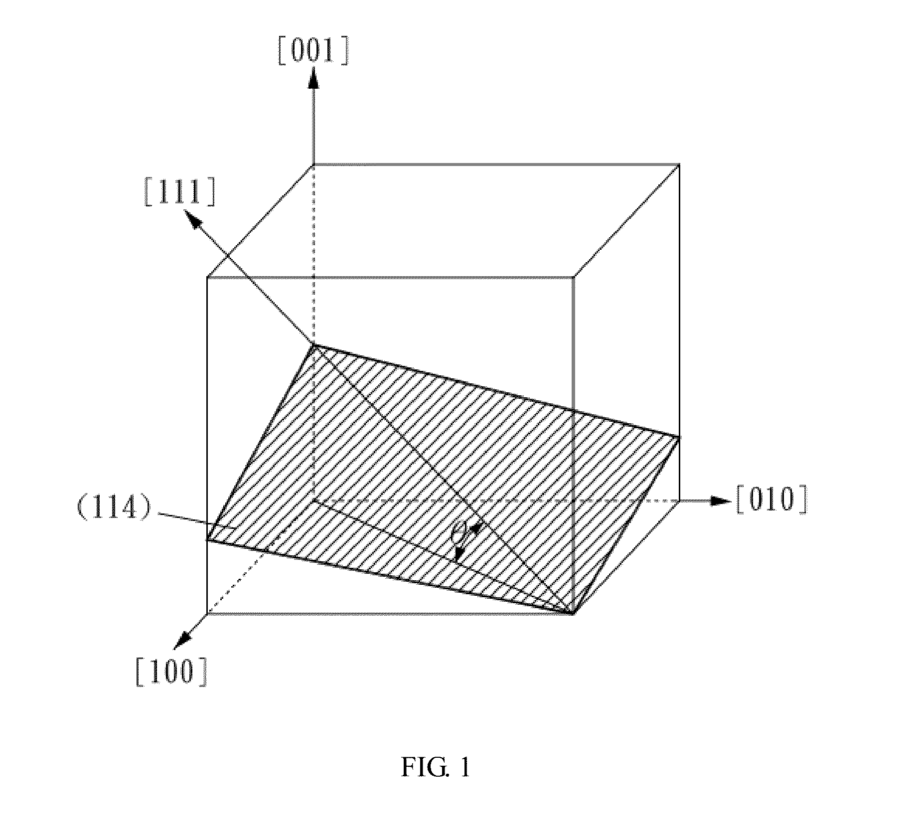
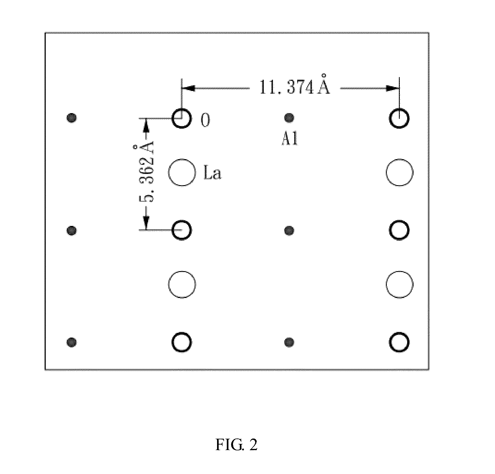
[0032]Next, referring to FIG. 1 and FIG. 2, FIG. 1 shows a schematic cross-section of plane (114) of the LaAlO3 (LAO) crystal having a miscut angle of about 19.47±1°, and FIG. 2 shows a schematic of the oxygen atom arrangement on the surface of the tangent plane (114) of the LaAlO3 (LAO) crystal. In the present embodiment, a LaAlO3 (LAO) crystal plane with a specific tangent plane is provided. After a plane (001) with a symmetry lattice constant is adjusted to an asymmetric plane (114), it has a unit length of 5.364 Å×11.367 Å as shown in FIG. 2. The crystal plane (114) is used as a substrate, which is cleaned with hot acetone and isopropanol and then placed in a vacuum chamber (a vacuum degree of 1×10⁻⁸ ton is maintained inside the chamber befo...

example 2

Growth of the Non-Polar (13 40) Crystal Plane of Nitride (III)

[0036]In this Example, the same procedure as disclosed in Example 1 is repeated except that the target material is replaced with Group III nitride, such as GaN. In Example 2, the Group III nitride epitaxy layer, such as GaN epitaxy layer, is deposited. The non-polar m plane of Group III nitride epitaxy layer, such as GaN epitaxy layer, grown by this Example may also achieve the same object and effect as that of Example 1.

[0037]In addition, although only GaN is given as an example, other target materials of Group III nitride, such as indium nitride, aluminum nitride, indium gallium nitride, aluminum gallium nitride, aluminum indium nitride, or aluminum indium gallium nitride etc., may also be used following the same procedure as in Example 1, to achieve the same object and effect.


PUM

PropertyMeasurementUnit
thicknessaaaaaaaaaa
miscut angleaaaaaaaaaa
temperatureaaaaaaaaaa

Abstract

The present invention relates to a method for growing a novel non-polar (13 40) plane epitaxy layer of wurtzite structure, which comprises the following steps: providing a single crystal oxide with perovskite structure; using a plane of the single crystal oxide as a substrate; and forming a non-polar (13 40) plane epitaxy layer of wurtzite semiconductors on the plane of the single crystal oxide by a vapor deposition process. The present invention also provides an epitaxy layer having non-polar (13 40) plane obtained according to the aforementioned method.

Description

BACKGROUND OF THE INVENTION[0001]1. Field of the Invention[0002]The present invention relates to a method for growing a non-polar (13 40) plane epitaxy layer of wurtzite structure semiconductors with a single crystal oxide as a substrate, particularly to a method for growing a non-polar (13 40) plane epitaxy layer of zinc oxide or Group III nitride with wide band gap, low lattice mismatch, and high thermal stability. The present invention also provides an epitaxy layer having a non-polar (13 40) plane.[0003]2. Description of Related Art[0004]GaN and its related nitrides have received great attention in recent years due to the successful application in solid light emitting devices and laser diodes. These nitrides belong to a wurtzite crystal structure of hexagonal crystal system, which mainly grows in a direction along c axis.[0005]Prior studies show that GaN grown in the direction along c axis may present a planar arrangement and induce a built-in electric field by polarization effe...

Claims


Application Information

Patent Timeline
Patent Type & Authority Applications(United States)
IPC IPC(8): C30B23/02C30B25/06C30B23/08C30B25/18H01L29/04C30B23/06
CPCC30B29/406H01L21/02631H01L21/02609C30B25/06H01L21/02554C30B29/16H01L29/045C30B25/18C30B23/066H01L21/0242C30B23/08C30B23/025H01L21/02433H01L29/2003H01L29/24C30B25/186
Inventor CHANG, LIHO, YEN-TENG
Owner NAT CHIAO TUNG UNIV
Learn More