High Speed Gallium Nitride Transistor Devices

a gallium nitride transistor, high-speed technology, applied in the direction of transistors, capacitors, semiconductor devices, etc., can solve problems such as adversely affecting other device properties

Active Publication Date: 2013-10-24
NXP USA INC
View PDF10 Cites 82 Cited by
  • Summary
  • Abstract
  • Description
  • Claims
  • Application Information

AI Technical Summary

Problems solved by technology

Attempts to reduce gate leakage current in such devices may adversely affect other device properties.

Method used


Image

  • High Speed Gallium Nitride Transistor Devices
  • High Speed Gallium Nitride Transistor Devices
  • High Speed Gallium Nitride Transistor Devices

Examples


Embodiment Construction

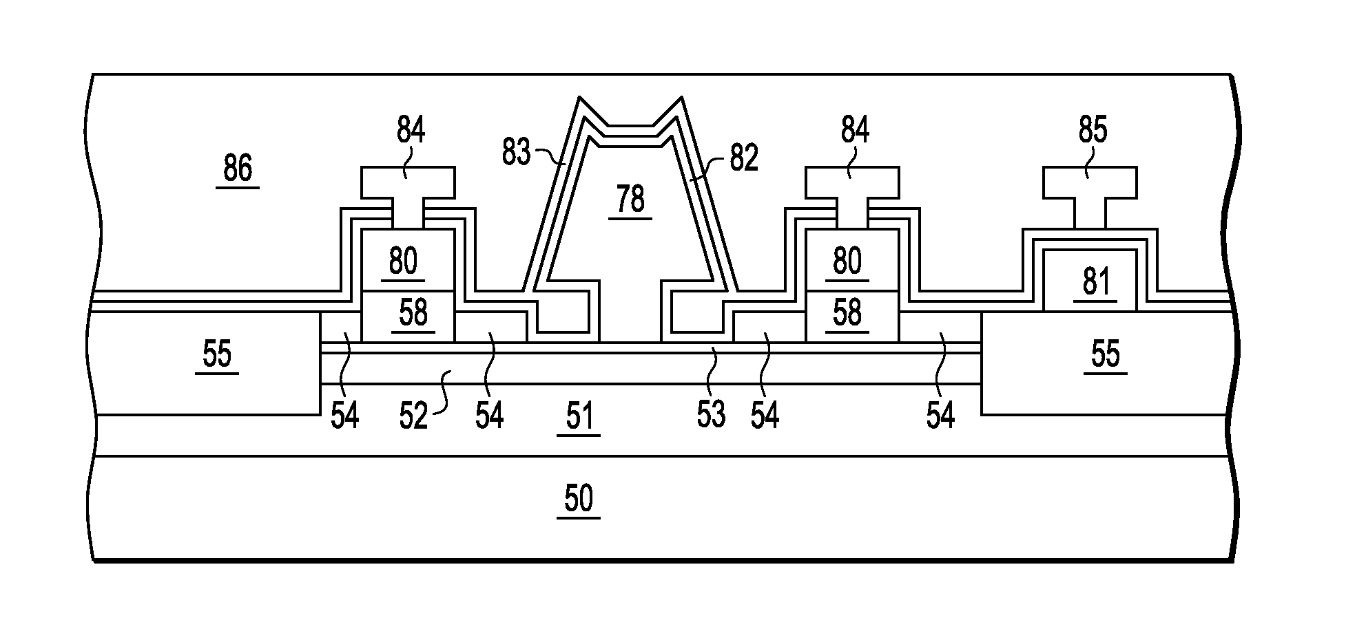
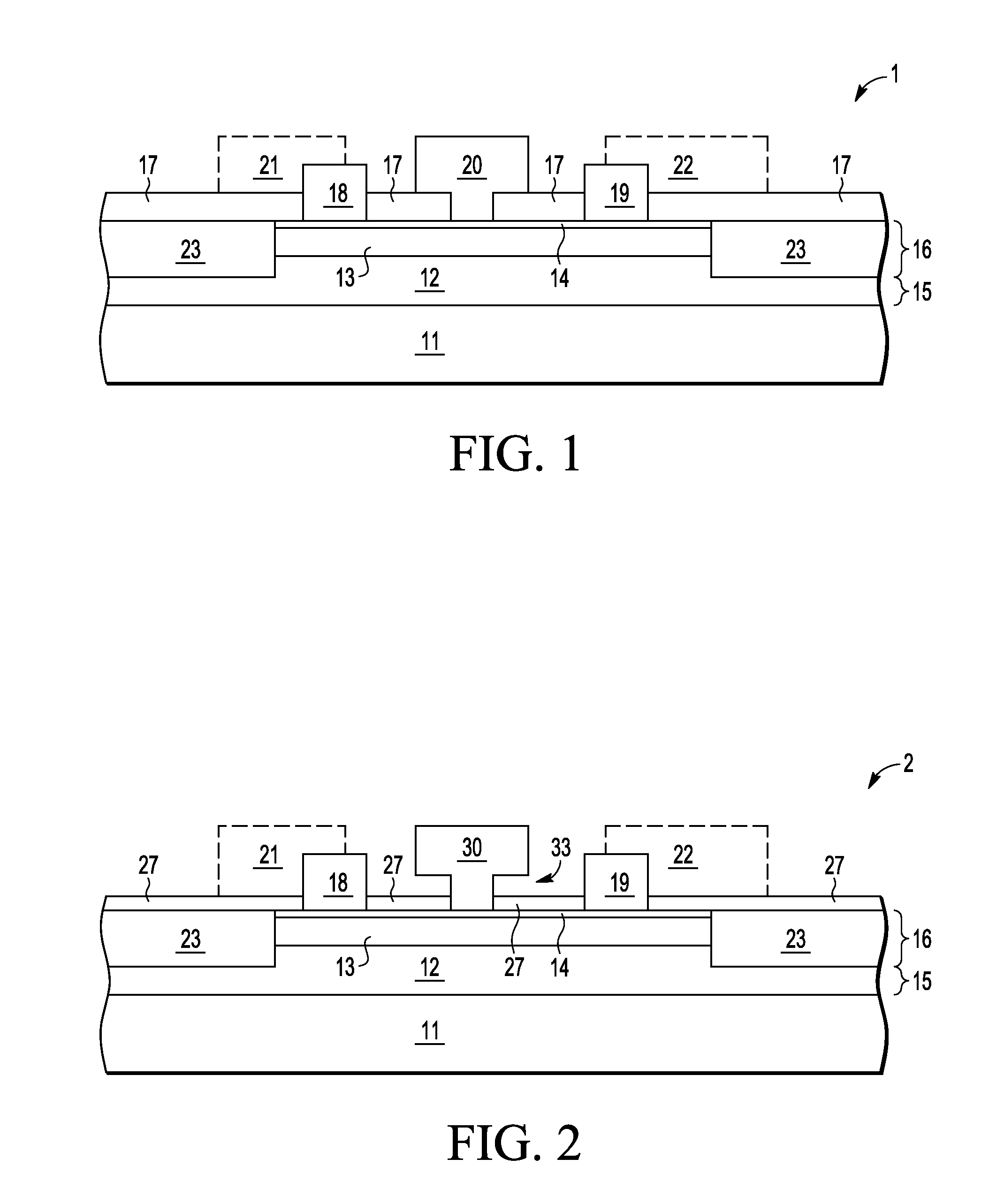
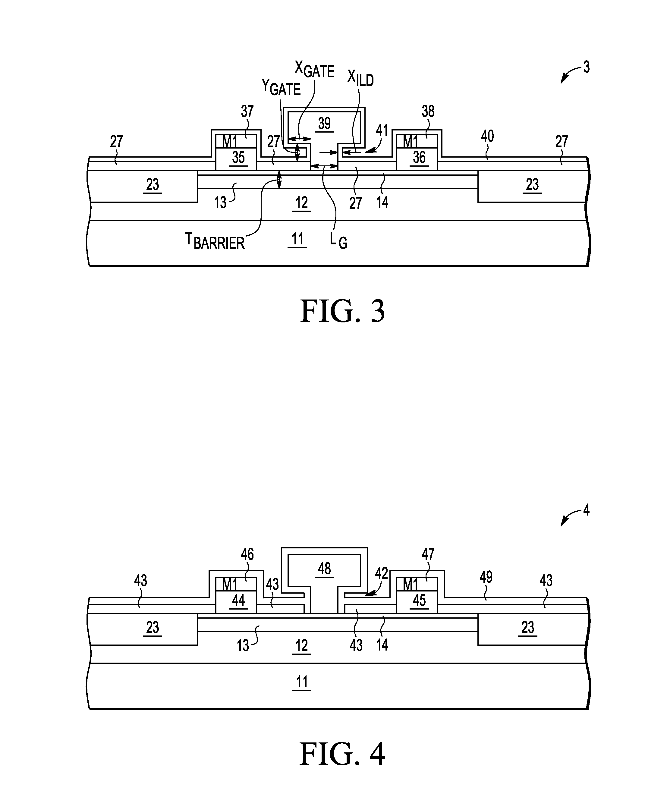
[0031]A high frequency, high voltage gallium nitride field effect transistor device and associated fabrication process are described for providing high unity current gain cut-off frequency (fT) and high maximum frequency of oscillation (fmax) with very low off-state gate and drain leakage currents by covering a gallium nitride substrate surface with a thin dielectric passivation layer e.g., 5-30 nm of LPCVD SiN) in which openings are etched to form gate and source / drain electrodes in ohmic contact with the gallium nitride substrate, where the gate electrode has sidewall extensions spaced apart from the thin dielectric passivation layer. During formation of the source / drain electrodes, a bottom capacitor plate may be formed with one or more patterned metal layers over an isolation region of the gallium nitride substrate. In selected embodiments, all or part of the sidewall surfaces of the gate electrode, source / drain electrodes, and bottom capacitor plate are coated by depositing one...


PUM


Abstract

A low leakage current switch device (110) is provided which includes a GaN-on-Si substrate (11-13) covered by a passivation surface layer (43) in which a T-gate electrode with sidewall extensions (48) is formed and coated with a conformal passivation layer (49) so that the T-gate electrode sidewall extensions are spaced apart from the underlying passivation surface layer (43) by the conformal passivation layer (49).

Description

BACKGROUND OF THE INVENTION[0001]1. Field of the Invention[0002]The present invention is directed in general to integrated circuit devices and methods for manufacturing same. In one aspect, the present invention relates to the manufacture and use of gallium nitride transistor devices.[0003]2. Description of the Related Art[0004]Semiconductor devices used in high-efficiency power amplifier (HEA) applications require higher speed and power handling capability. To meet these operating requirements, high power semiconductor devices may be formed with semiconductor materials, such as gallium nitride (GaN) having material properties that are suitable for use in such applications. For example, high speed transistor switch devices, such as high electron mobility transistor (HEMT) devices, formed with GaN-based materials offer many advantages in RF applications, especially in HEA applications, by delivering high current, high breakdown voltage, and high unity gate current cutoff frequency (f...

Claims


Application Information

Patent Timeline
Patent Type & Authority Applications(United States)
IPC IPC(8): H01L29/20H01L21/336
CPCH01L29/7787H01L27/0629H01L28/60H01L29/2003H01L29/402H01L29/404H01L29/42316H01L29/42376H01L29/475H01L29/66462
Inventor GREEN, BRUCE M.MOORE, KAREN E.HARTIN, OLIN
Owner NXP USA INC
Why Eureka
Try Eureka