Microfluidic electrochemical device and process for chemical imaging and electrochemical analysis at the electrode-liquid interface in-situ
a microfluidic electrochemical and electrode liquid technology, applied in the direction of material electrochemical variables, instruments, and phase/state change investigations, can solve the problems of inability to accurately analyze the electrode-solution interface in-situ, emersion adlayers may only partially or incompletely represent the real in-situ system, and the in-situ chemical imaging of the actual electrode-electrolyte interface has not yet been achieved
- Summary
- Abstract
- Description
- Claims
- Application Information
AI Technical Summary
Benefits of technology
Problems solved by technology
Method used
Image
Examples
example 1
Microfluidic Electrochemical Cell
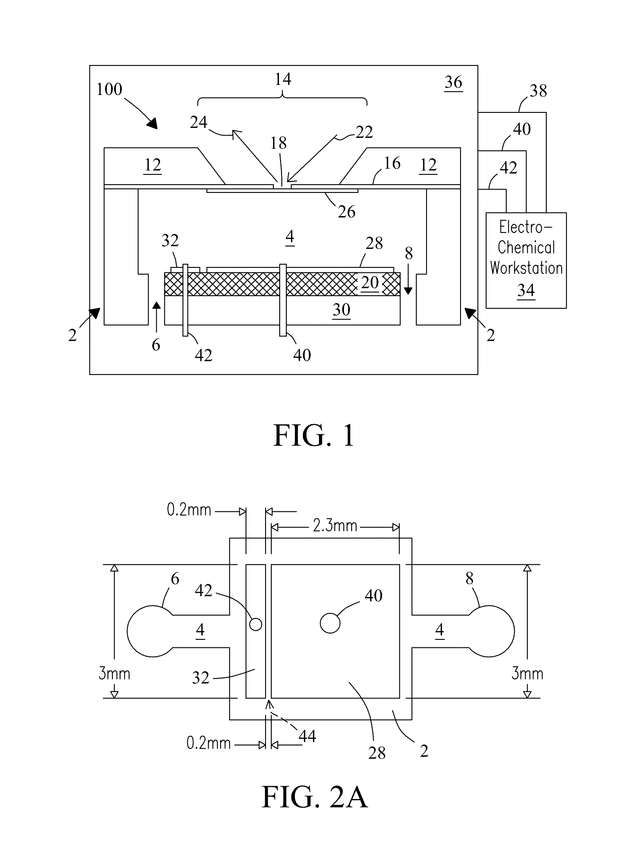
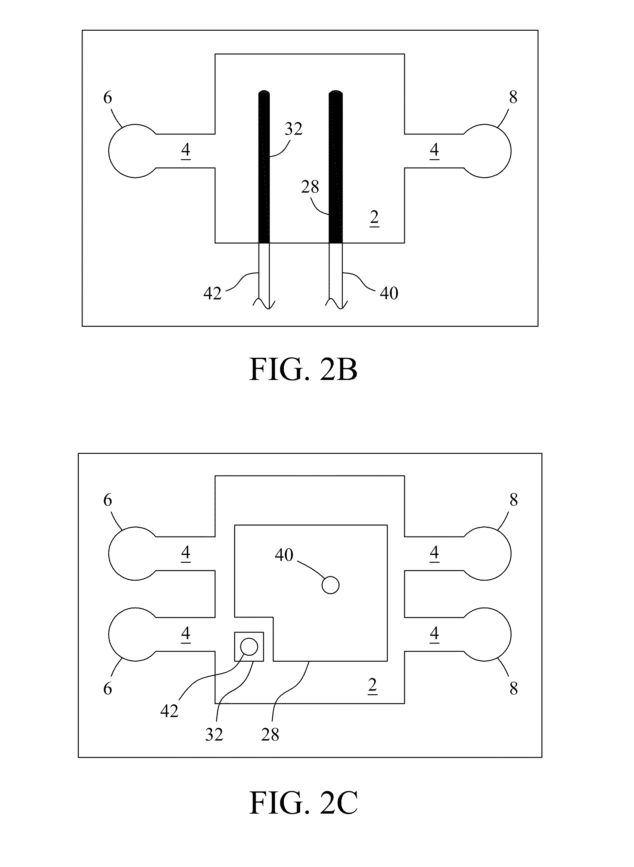
[0061]The microfluidic electrochemical device was fabricated using a soft lithography approach. Exemplary dimensions of the electrochemical flow chamber were approximately 2.5 mm×2.5 mm×0.3 mm. The photomask was designed using AutoCAD software and printed with a mask printer (Intelligent Micro Patterning LLC, Model SF-100 Xpress). A template for casting the electrochemical flow chamber was made with SU-8 photoresist (Microchem, Newton, Mass.) on a silicon substrate. The template included a flow channel with a depth of 300 μm equal to the distance between the working electrode and a counter electrode. A 10:1 ratio (w / w) of polydimethylsiloxane (PDMS) prepolymer and curing agent (Sylgard 184, Dow Corning Co., Midland, Mich., USA) were thoroughly mixed, degassed under vacuum, poured onto the patterned template to a thickness of 1 cm, and cured in an oven at 75° C. overnight.
example 2
Preparation of Potassium Iodide Sample Solutions
[0062]Aqueous 10 mM solutions of potassium iodide (Aldrich, 99.9%) were prepared in ultrapure water (18.2 MΩ·cm) obtained with a water purification system (Milli-Q Integral Water Purification System, EMD Millipore, Billerica, Mass., USA) at 25° C. Oxygen in the solutions was depleted using a nitrogen bubbler before filling the microfluidic electrochemical device. Solutions were degassed using a commercial degasser (e.g., a DU series 200 μL Degasys Ultimate internal volume degasser, Sanwa Tsusho Co., Ltd., Tokyo, Japan) to limit pressure build-up and bubble formation inside the device. The microfluidic electrochemical device was filled with solution using a syringe pump (Harvard apparatus, Holliston, Mass., USA).
example 3
Operation in ToF-SIMS
[0063]The vacuum compatible microfluidic electrochemical device was deployed into a vacuum chamber of a commercial ToF-SIMS instrument (IONTOF GmbH, Munster, Germany). The microfluidic electrochemical device was checked for leaks in a vacuum chamber before usage. Vacuum pressure in the flow chamber of the electrochemical device during measurements was 2.0×10⁻⁷ Torr to 5.5×10⁻⁷ Torr. The ToF-SIMS instrument was configured to raster a focused (0.2 μm) primary ion beam through the SiN window of the electrochemical device over sample liquids. Ejected secondary ions were mass-analyzed to form surface chemical maps with a lateral resolution of about 0.2 μm. ToF-SIMS measurements were performed at a beam current of ˜1.0 pA with a beam width of 125 ns and a repeated frequency of 16.7 kHz. ToF-SIMS provides molecular information, e.g., on the top layer (e.g., ˜6 nm) of sample liquids and other solutions. ToF-SIMS may employ, e.g., 25 keV Bi+ ions as probes. Ions were det...
PUM
 Abstract
Description
Claims
Application Information


