Semiconductor device and manufacturing method thereof

a technology of semiconductor devices and semiconductor devices, applied in the direction of semiconductor devices, electrical equipment, transistors, etc., can solve the problems of reducing the reliability of semiconductor devices that use transistors, and achieve the effect of increasing the reliability of semiconductor devices and stable characteristics

Active Publication Date: 2014-02-13
SEMICON ENERGY LAB CO LTD
View PDF1 Cites 99 Cited by
  • Summary
  • Abstract
  • Description
  • Claims
  • Application Information

AI Technical Summary

Benefits of technology

[0024]With one embodiment of the present invention, a transistor having electrically stable characteristics can be provided. By using the transistor in a semiconductor device, the reliability of the semiconductor device can be increased.

Problems solved by technology

There is a problem in transistors including an oxide semiconductor in that electrical characteristics, typically the threshold voltage, vary with time or by bias-temperature stress test (also referred to as gate bias temperature (GBT) test).
Such a variation in electrical characteristics of the transistor is a cause of a reduction in the reliability of a semiconductor device that uses the transistor.

Method used


Image

  • Semiconductor device and manufacturing method thereof
  • Semiconductor device and manufacturing method thereof
  • Semiconductor device and manufacturing method thereof

Examples


embodiment 1

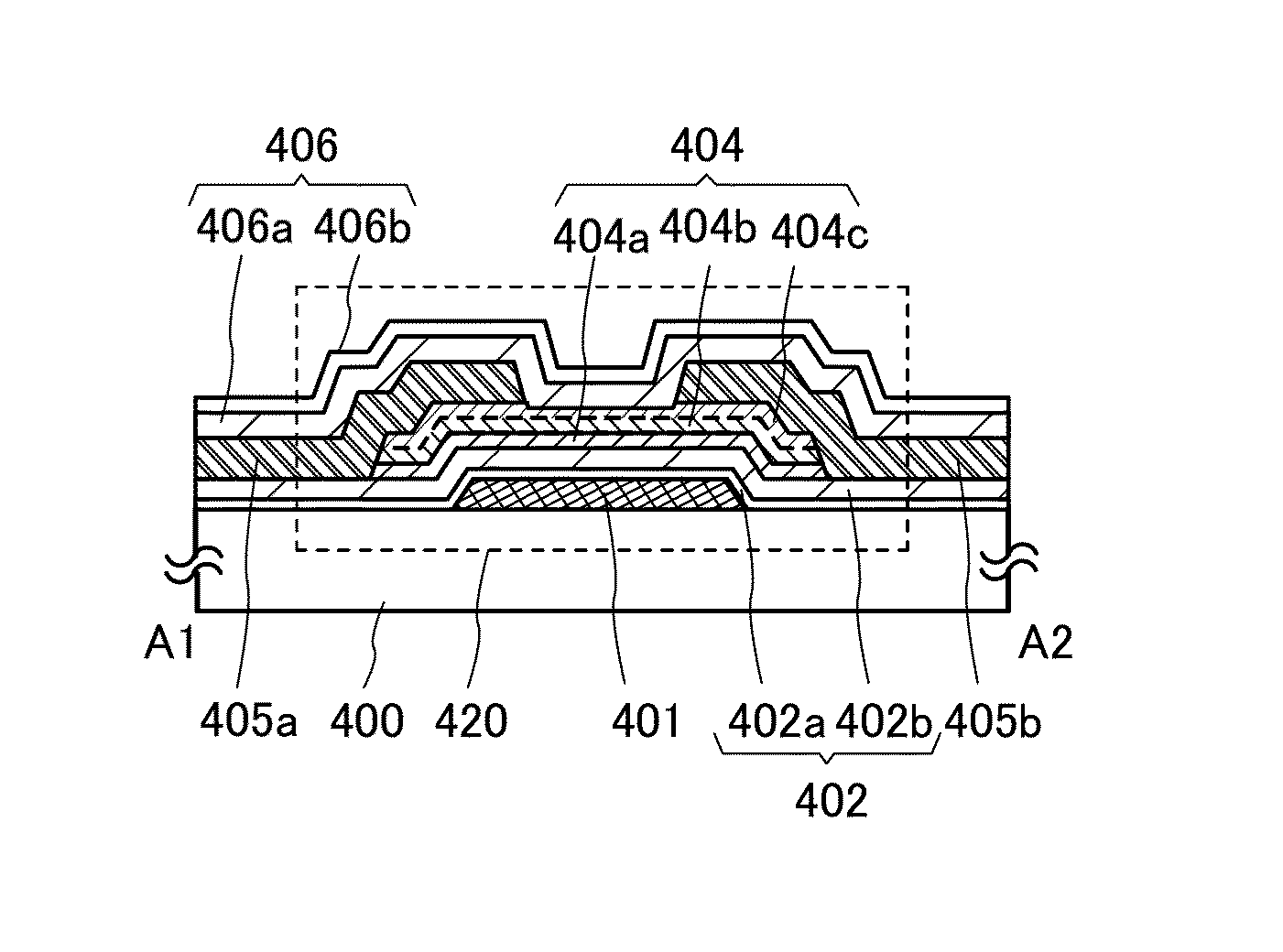
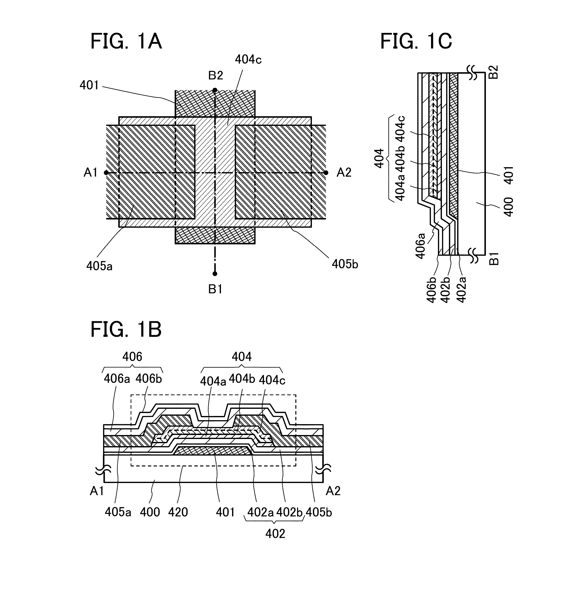
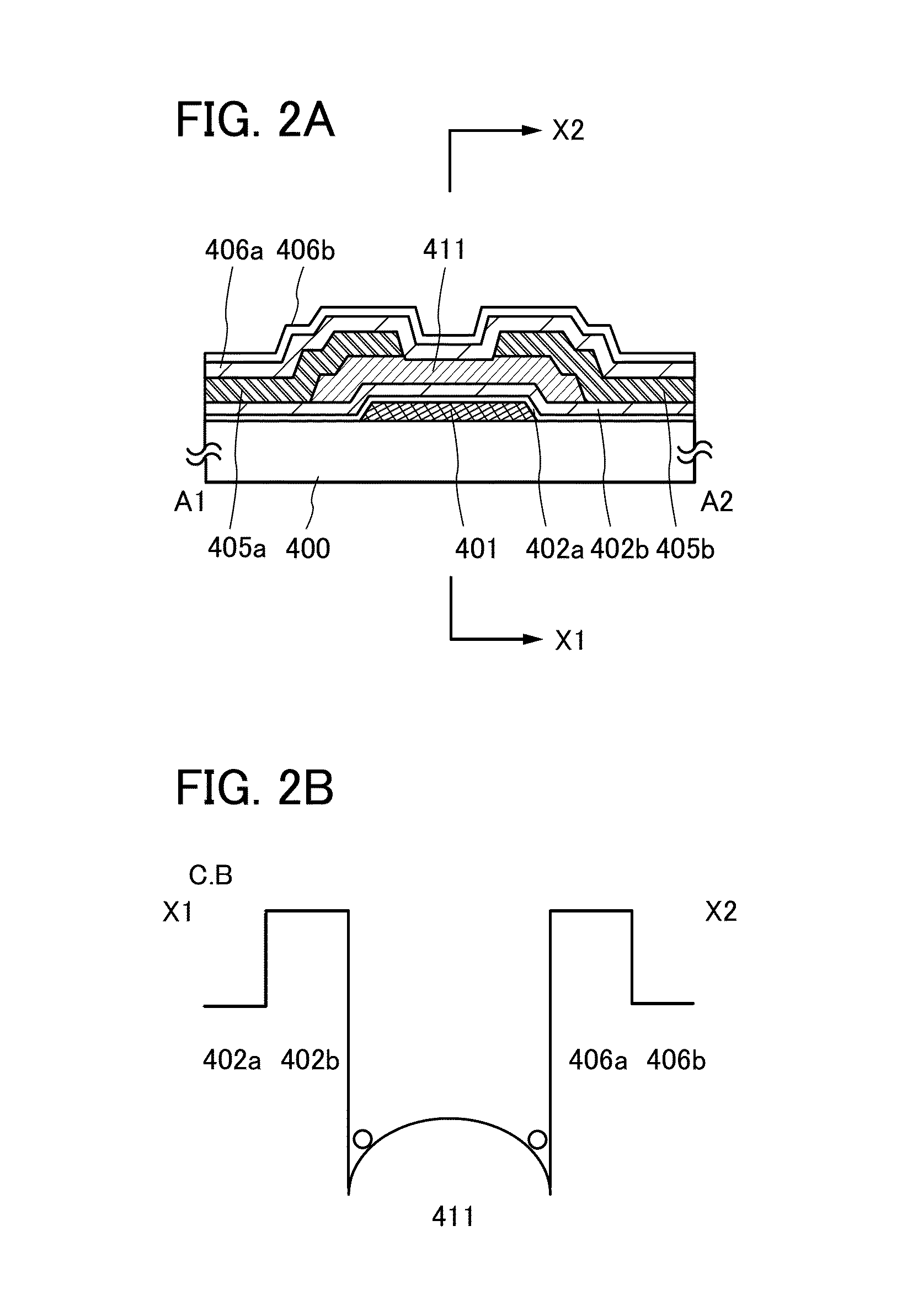
[0046]In this embodiment, a mode of a semiconductor device according to one embodiment of the present invention will be described with reference to FIGS. 1A to 1C, FIGS. 2A and 2B, FIGS. 3A to 3C, and FIGS. 4A to 4D.

[0047]There is no particular limitation on the structure of a transistor that is provided in the semiconductor device according to one embodiment of the present invention; for example, a staggered type or a planar type having a top-gate structure or a bottom-gate structure can be employed. Further, the transistor may have a single gate structure including one channel formation region, or a multi-gate structure such as a double gate structure including two channel formation regions or a triple gate structure including three channel formation regions. Further, the transistor may have a dual-gate structure including two gate electrode layers positioned above and below a channel formation region with gate insulating films interposed therebetween.

[0048]FIGS. 1A to 1C illustra...

embodiment 2

[0137]In this embodiment, a method for manufacturing the transistor including the oxide semiconductor stacked film illustrated in FIGS. 1A to 1C will be described with reference to FIGS. 5A to 5E.

[0138]First, the gate electrode layer 401 is formed over the substrate 400 (see FIG. 5A).

[0139]There is no particular limitation on the substrate that can be used as the substrate 400 having an insulating surface as long as it has at least heat resistance to withstand heat treatment performed later. For example, a variety of glass substrates for electronics industry, such as a barium borosilicate glass substrate or an aluminoborosilicate glass substrate can be used. Note that as the substrate, a substrate having a thermal expansion coefficient of greater than or equal to 25×10−7 / ° C. and less than or equal to 50×10−7 / ° C. (preferably greater than or equal to 30×10−7 / ° C. and less than or equal to 40×10−7 / ° C.) and a strain point of higher than or equal to 650° C. and lower than or equal to ...

embodiment 3

[0232]A semiconductor device having a display function (also referred to as a display device) can be manufactured using any of the transistors described in Embodiment 1. Further, part or all of the driver circuitry which includes the transistor can be formed over a substrate where a pixel portion is formed, whereby a system-on-panel can be formed.

[0233]In FIG. 9A, a sealant 4005 is provided so as to surround a pixel portion 4002 provided over a substrate 4001, and the pixel portion 4002 is sealed with a substrate 4006. In FIG. 9A, a scan line driver circuit 4004 and a signal line driver circuit 4003 which are each formed using a single crystal semiconductor film or a polycrystalline semiconductor film over an IC chip or a substrate separately prepared are mounted on the substrate 4001, in a region which is different from the region surrounded by the sealant 4005. Various signals and potentials which are provided to the pixel portion 4002 through the signal line driver circuit 4003 a...


PUM


Abstract

The present invention provides a transistor having electrically stable characteristics. In addition, the reliability of a semiconductor device including such a transistor is increased. The semiconductor device includes a gate electrode layer, a gate insulating film over the gate electrode layer, an oxide semiconductor stacked film overlapping with the gate electrode layer with the gate insulating film provided therebetween, and a pair of electrode layers in contact with the oxide semiconductor stacked film. In the semiconductor device, the oxide semiconductor stacked film includes at least indium and includes a first oxide semiconductor layer, a second oxide semiconductor layer, and a third oxide semiconductor layer which are sequentially stacked. Further, the first oxide semiconductor layer has an amorphous structure, the second oxide semiconductor layer and the third oxide semiconductor layer include a crystal part whose c-axis is substantially perpendicular to a top surface of the oxide semiconductor stacked film.

Description

TECHNICAL FIELD[0001]The present invention relates to a semiconductor device including a field-effect transistor including an oxide semiconductor stacked film and a manufacturing method thereof.BACKGROUND ART[0002]Transistors used for most flat panel displays typified by a liquid crystal display device and a light-emitting display device are formed using silicon semiconductors such as amorphous silicon, single crystal silicon, and polycrystalline silicon provided over glass substrates. Further, transistors formed using such silicon semiconductors are used in integrated circuits (ICs) and the like.[0003]In recent years, attention has been drawn to a technique in which, instead of a silicon semiconductor, a metal oxide exhibiting semiconductor characteristics is used in transistors. Note that in this specification and the like, a metal oxide exhibiting semiconductor characteristics is referred to as an oxide semiconductor.[0004]For example, such a technique is disclosed that a transis...

Claims


Application Information

Patent Timeline
Patent Type & Authority Applications(United States)
IPC IPC(8): H01L29/786
CPCH01L29/78693H01L29/7869H01L29/78606H01L27/1225H01L29/045H01L29/1037
Inventor YAMAZAKI, SHUNPEI
Owner SEMICON ENERGY LAB CO LTD
Why Eureka
Try Eureka