Silk transistor devices

Active Publication Date: 2014-04-03
TUFTS UNIV
View PDF2 Cites 23 Cited by
  • Summary
  • Abstract
  • Description
  • Claims
  • Application Information

AI Technical Summary

Benefits of technology

[0011]Another aspect of the invention relates to methods of fabrication a silk-based electronic device. The method comprises the steps of providing an electrically active layer comprising an organic semiconducting material; and providing a substrate to support the active layer. The method may further comprise applying a dielectric layer to the substrate between the active layer and substrate. The substrate and dielectric layer may be a silk matrix or silk matrix combining with other conventional plastic materials. The m

Problems solved by technology

This is a fundamental issue for an effective paradigm shift to a low co

Method used


Image

  • Silk transistor devices
  • Silk transistor devices
  • Silk transistor devices

Examples


example 1

Silk-Based n-Type Field Effect Transistor

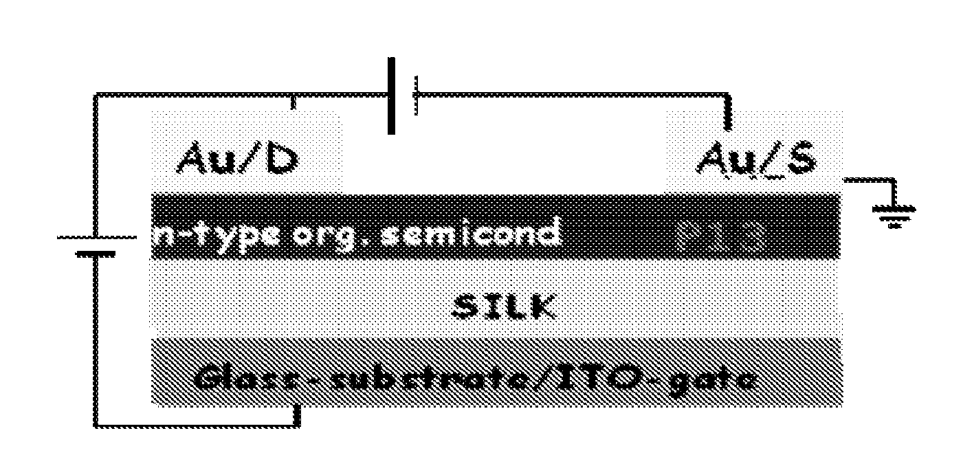
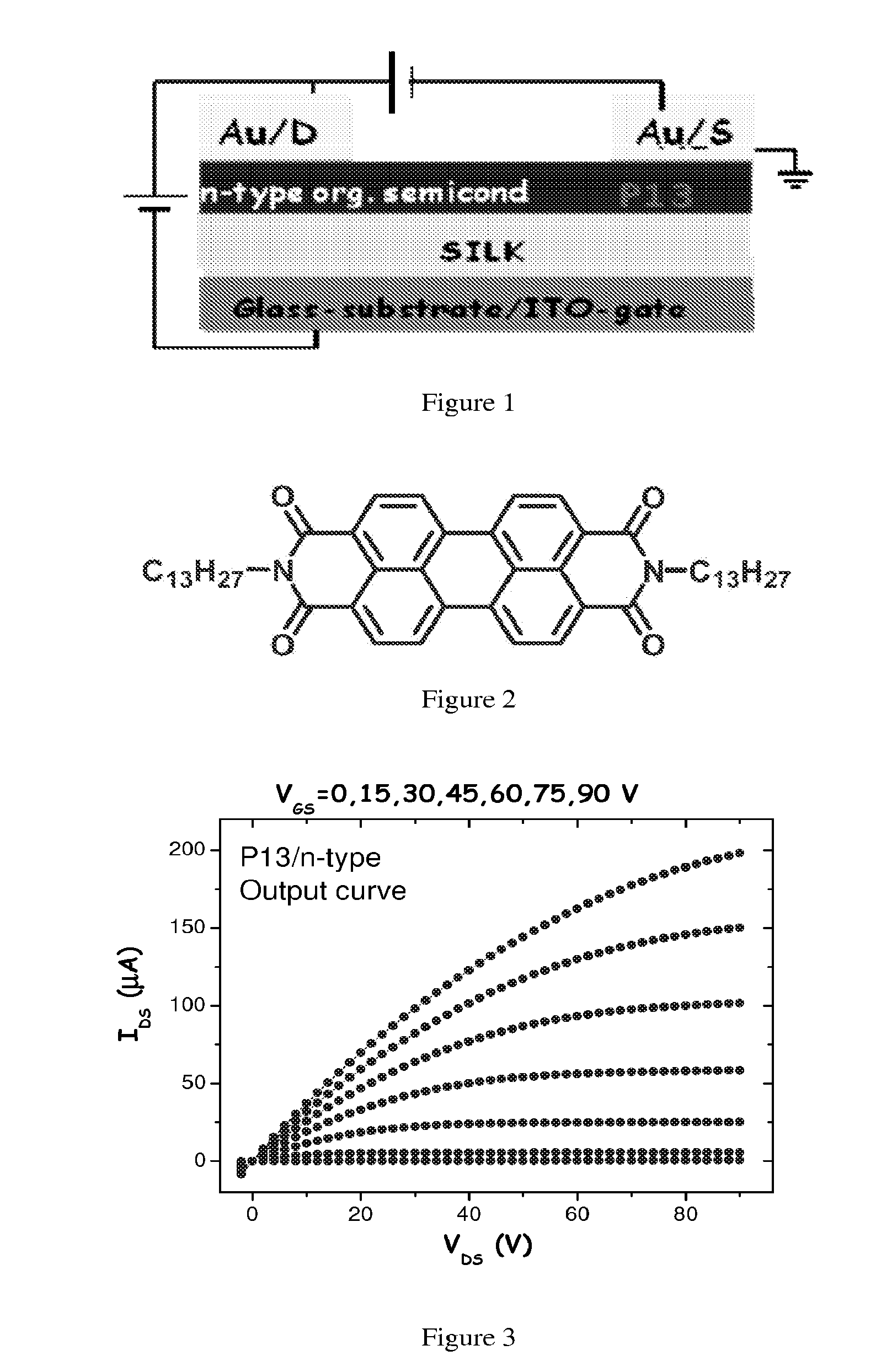
[0202]FIG. 1 shows a top configuration of typical field effect transistor architecture. Silk fibroin solution (7% w / v) was used to spin coat a crosslinked silk dielectric film (−600 nm) onto a glass / patterned indium-tin-oxide (ITO) (transparent substrate / gate) substrate, with a patterned ITO acting as a gate contact. On top of the silk film, a prototypical n-type semiconducting compound for electron conduction, namely the N,N′-ditridecylperylene-3,4,9,10-tetracarboxylic diimide (P13) (molecular structure shown in FIG. 2), was vacuum-deposited at a sublimation rate of 0.1 Å / s until a thickness of 15 nm was reached. A 50 nm-thick source and drain gold contacts were vacuum thermo-deposited through a metal mask completing a typical top-contact organic field-effect transistor (OFET) configuration.

[0203]The silk-based transistor can be operated and characterized by a probe station equipped with a parametric analyzer both in atmosphere controlled dr...

example 2

Silk-Based p-Type Field Effect Transistor

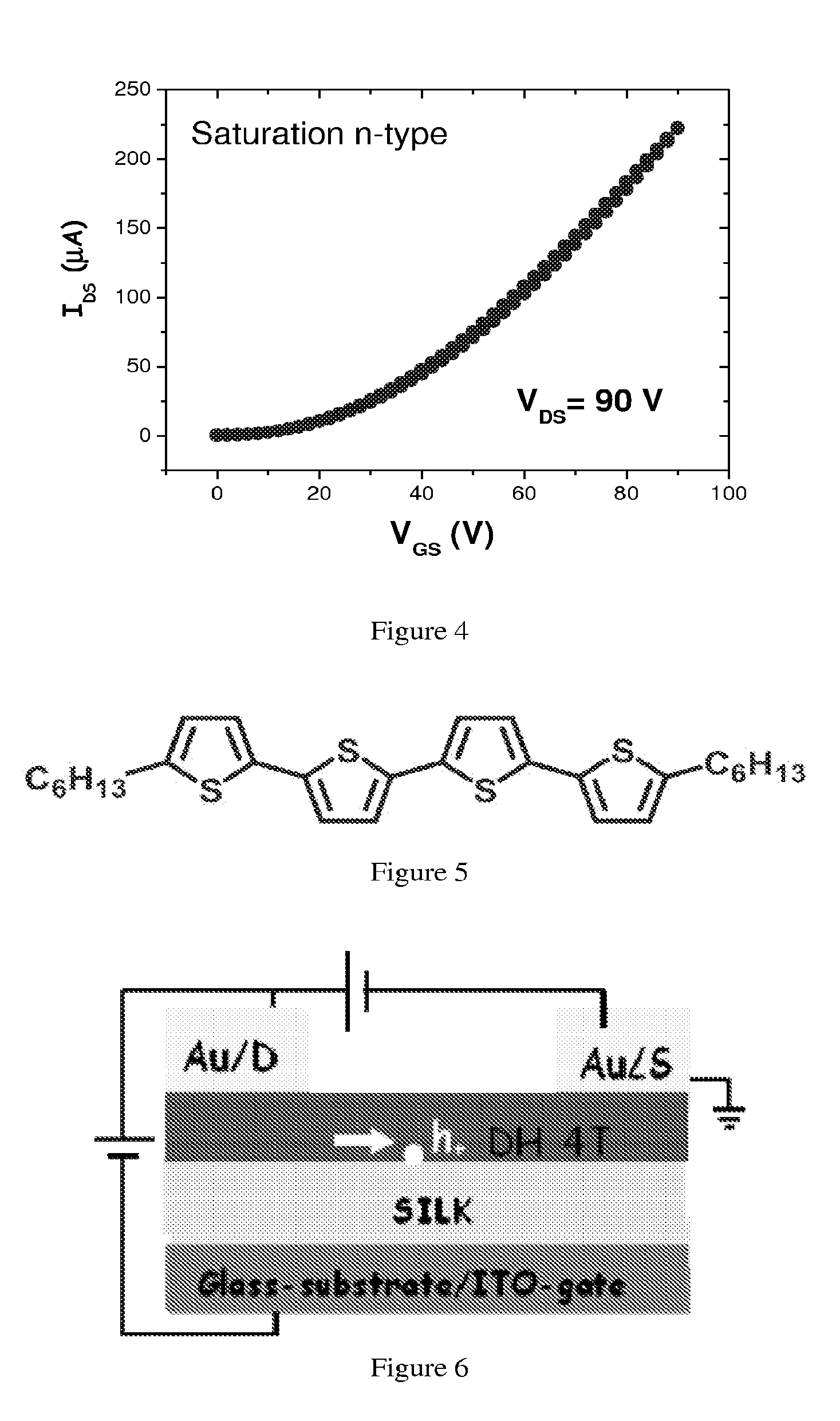
[0207]Similarly to the manner the silk-based n-type transistor was fabricated, a p-type silk-based transistor in the top contact configuration was fabricated as shown in FIG. 6. Silk fibroin solution (7% w / v) was used to spin coat a crosslinked silk dielectric film (˜600 nm) onto a glass / patterned indium-tin-oxide (ITO) (transparent substrate / gate) substrate, with a patterned ITO acting as a gate contact. On top of the silk film, a prototypical p-type semiconducting compound, namely the α,ω-dihexyl-quaterthiophene (DH4T) (molecular structure as shown in FIG. 5), was vacuum-deposited at a sublimation rate of 0.1 Å / s until a thickness of 15 nm was reached. A 50 nm-thick source and drain gold contacts were vacuum thermo-deposited through a metal mask completing a typical top-contact organic field-effect transistor (OFET) configuration.

[0208]Following similar methodology described above for silk-based n-type transistor, the silk-based p-type tran...

example 3

Silk-Living Cell Electronic Device

[0211]A silk-gel may be obtained via the physical crosslinking of the hydrophobic domains in the silk, resulting in beta sheet crosslinks. These interactions stabilize the silk, resulting in insolubility in aqueous systems.

[0212]A preparation of astroglial primary cells may be added with a standard physiological saline buffer solution. The cells entered the silk-gel matrix maintaining viability over 2 months under ambient conditions. The demonstration of bioactive features of the silk-gel system with primary astroglial cells was confirmed by confocal microscopy as shown in FIG. 11.

[0213]The silk-gel systems infiltrated with physiological saline solution and the astroglial cells were moved to the top of the device. For comparison, blank control samples were prepared following the same protocol of fabrication and manipulation, with the silk-gel and the physiological saline solution in absence of the cells. Operating the device with a drain-source volt...


PUM

PropertyMeasurementUnit
Electrical conductoraaaaaaaaaa
Transport propertiesaaaaaaaaaa
Biocompatibilityaaaaaaaaaa

Abstract

The invention relates to ecosustainable and biocompatible, low cost, ambient friendly electronic and optoelectronic devices, such as transistors and light-emitting transistors, made with silk fibroin or blended with other biopolymers, methods for fabrication and methods of using the silk-based electronics and optoelectronics. The silk-based electronics and optoelectronics can be implanted in vivo and in vitro for biomedical applications, such as for drug discovery or drug screening assays and devices. The silk-based devices may be used in the food industry and embedded in packaging for tracking and sensing, for security purposes or exploited as disposable not harmful for the environment efficient general electronic and optoelectronic devices.

Description

CROSS REFERENCE TO RELATED APPLICATION[0001]This application claims benefit of priority under 35 U.S.C. §119(e) of U.S. Provisional Application No. 61 / 238,319 filed Aug. 31, 2009, the contents of which are incorporated herein by reference in its entirety.GOVERNMENT SUPPORT[0002]This invention was made with government support under contract No. W911NF-07-1-0618 awarded by the U.S. Army Research Laboratory and the U.S. Army Research Office. The U.S. federal government has certain rights in the invention.FIELD OF THE INVENTION[0003]The invention is directed to ecosustainable and biocompatible, low cost, ambient friendly electronic or optoelectronic devices made with silk fibroin or combined with other biopolymers, methods for fabrication and methods of using thereof.BACKGROUND OF THE INVENTION[0004]Recently, innovative devices based on semiconductors (Rogers & Huang, 27 PNAS 10875-76 (2009); Kim & Rogers, 20 Adv. Mater. 4887-92 (2008)) have been developed. In particular, attempts have ...

Claims


Application Information

Patent Timeline
IPC IPC(8): H01L51/00H01L51/05H01L51/52G01N33/50
CPCH01L51/0093G01N33/502H01L51/0545H01L51/5296H01L51/052B82Y10/00B82Y5/00C07K14/43586H10K85/621H10K85/113H10K85/761H10K10/471H10K10/486H10K10/488H10K10/466H10K50/30
Inventor OMENETTO, FIORENZOKAPLAN, DAVID L.AMSDEN, JASONCAPELLI, RAFFAELLATOFFANIN, STEFANOBENFENATI, VALENTINAMUCCINI, MICHELEZAMBONI, ROBERTO
Owner TUFTS UNIV
Why Eureka
Try Eureka