Direct growth of graphene films on non-catalyst surfaces

a graphene film, non-catalyst technology, applied in the direction of physical/chemical process catalysts, metal/metal-oxide/metal-hydroxide catalysts, vacuum evaporation coating, etc., can solve the problems of various limitations of current methods for forming graphene films

Inactive Publication Date: 2014-05-01
RICE UNIV
View PDF2 Cites 128 Cited by
  • Summary
  • Abstract
  • Description
  • Claims
  • Application Information

AI Technical Summary

Benefits of technology

[0010]As set forth in more detail below, the methods of the present invention provide numerous advantages, including the direct formation of homogenous graphene films on a desired surface without the need for a transfer step. As also set forth in more detail below, the graphene films formed by the methods of the present invention can find numerous applications in various fields.

Problems solved by technology

Current methods to form graphene films suffer from various limitations.

Method used


Image

  • Direct growth of graphene films on non-catalyst surfaces
  • Direct growth of graphene films on non-catalyst surfaces
  • Direct growth of graphene films on non-catalyst surfaces

Examples


example 1

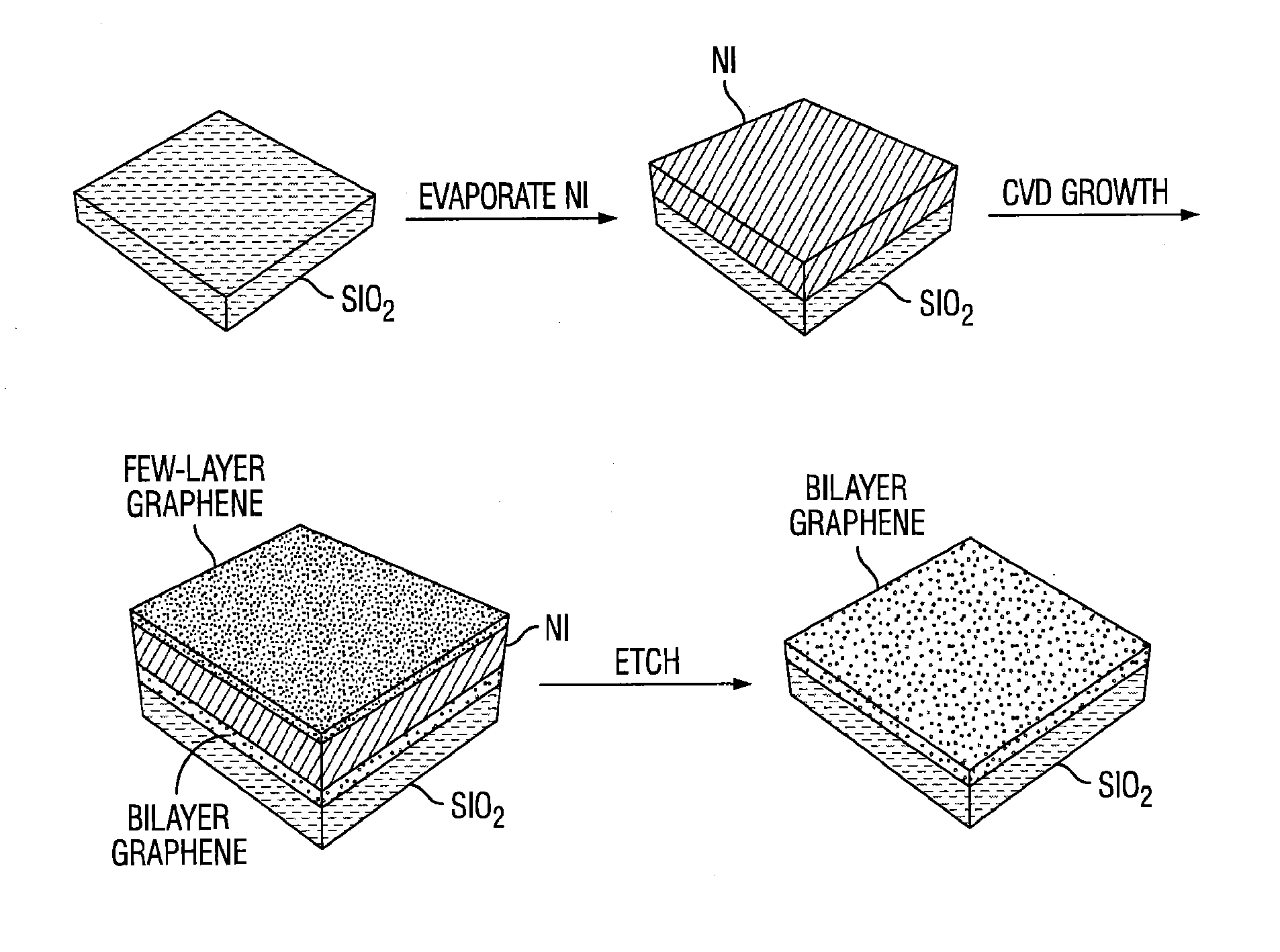
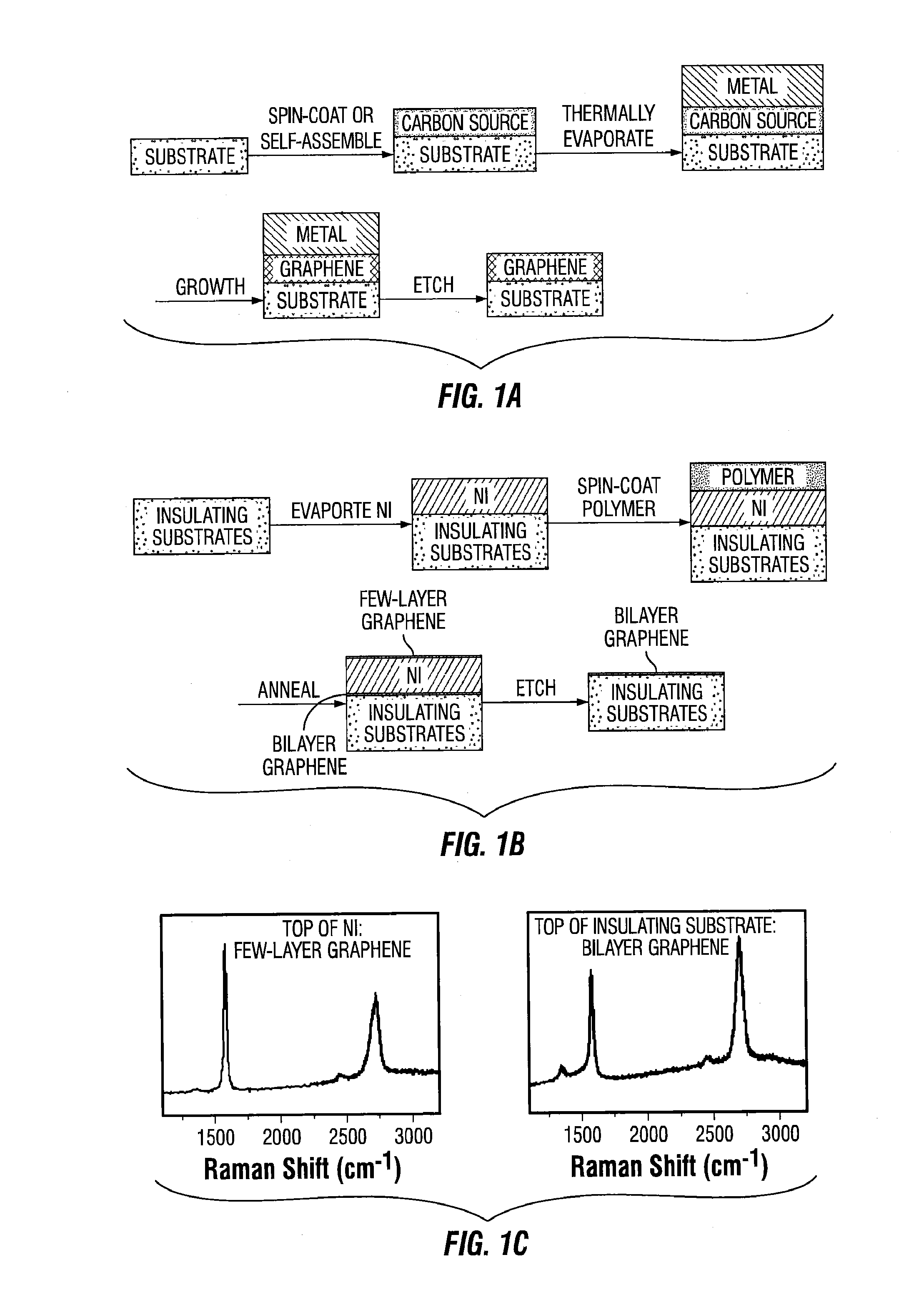
Direct Growth of Bilayer Graphene on Insulating Substrates

[0111]Since its first isolation in 2004, graphene has garnered enormous interest because of its promising electronic applications. Bilayer graphene is particularly interesting because it has a tunable bandgap, thereby being more attractive for many electronic and optical device embodiments. For such applications, uniform-thickness and large-size bilayer graphene films on insulating substrates are desirable. However, the present growth methods either need an additional lift-off step to transfer graphene from the metal catalyst surfaces to the insulating substrates, such as in chemical vapor deposition (CVD) and solid carbon source synthesis methods, or they have difficulty yielding uniform bilayer graphene films directly on insulating substrates, as in epitaxial growth methods from SiC.

[0112]Here, we demonstrate a general transfer-free method to directly grow large areas of uniform bilayer graphene on insulating substrates (e....

example 1.1

Methods Summary

[0134]The Ni film was deposited via an Edwards Auto 306 Thermal Evaporator. Raman spectroscopy was performed with a Renishaw RE02 Raman microscope using 514-nm laser excitation at room temperature. A 2100F field emission gun transmission electron microscope was used to take the high-resolution TEM images of graphene samples transferred onto a lacey carbon (Ted Pella) or a C-flat TEM grid (Protochips). Electrical characterizations were performed using an Agilent 4155C semiconductor parameter analyzer at room temperature at 106 Torr. XPS was performed on a PHI Quantera SXM scanning X-ray microprobe with 100 □m beam size and 45° takeoff angle. The thickness of SAMs was determined using an LSE Stokes ellipsometer with a He—Ne laser light source at a λ of 632.8 nm of an angle of incidence of 70°.

example 1.2

Cleaning of Insulating Substrates

[0135]Prior to coating the insulating substrates with the solid carbon sources, the SiO2 underwent a surface cleaning by oxygen-plasma etching for 10 min, followed by immersion in piranha solution (4:1 sulfuric acid:hydrogen peroxide) at 95° C. for 30 min. The substrates were placed in DI water and sonicated (Fisher Scientific FS110H) for more than 60 min. The SiO2 surfaces were thoroughly rinsed with DI water and were dried by a nitrogen flow. The substrates were further dried in a vacuum oven (˜100 Torr) at 80° C. for 30 min. The h-BN substrates were made by transferring CVD-grown h-BN layers to cleaned SiO2 / Si. Before spin-coating the polymer film, h-BN / SiO2 / Si substrates were annealed for 60 min at 400° C. with H2 (50 sccm) / Ar (500 sccm) and reduced pressure (˜7.0 Torr). A 500-nm-layer of Si3N4 was grown on SiO2 / Si++ substrates having a 500-nm-thick SiO2 layer using plasma-enhanced chemical vapor deposition (PECVD). Both Si3N4 and sapphire were c...


PUM

PropertyMeasurementUnit
temperatureaaaaaaaaaa
thickaaaaaaaaaa

Abstract

The present invention provides methods of forming graphene films on various non-catalyst surfaces by applying a carbon source and a catalyst to the surface and initiating graphene film formation. In some embodiments, graphene film formation may be initiated by induction heating. In some embodiments, the carbon source is applied to the non-catalyst surface before the catalyst is applied to the surface. In other embodiments, the catalyst is applied to the non-catalyst surface before the carbon source is applied to the surface. In further embodiments, the catalyst and the carbon source are applied to the non-catalyst surface at the same time. Further embodiments of the present invention may also include a step of separating the catalyst from the formed graphene film, such as by acid etching.

Description

CROSS REFERENCE TO RELATED APPLICATIONS[0001]This application claims priority to U.S. Provisional Patent Application No. 61 / 478,672, filed on Apr. 25, 2011. The entirety of the above-referenced provisional application is incorporated herein by reference.STATEMENT REGARDING FEDERALLY SPONSORED RESEARCH[0002]This invention was made with government support under the Office of Naval Research Grant No. N00014-09-1-1066, awarded by the U.S. Department of Defense; and the Air Force Office of Scientific Research Grant No. FA9550-09-1-0581, also awarded by the U.S. Department of Defense. The government has certain rights in the invention.BACKGROUND OF THE INVENTION[0003]Graphene films find many applications in various fields. Current methods to form graphene films suffer from various limitations. Therefore, there is currently a need to develop more optimal methods of forming graphene films.BRIEF SUMMARY OF THE INVENTION[0004]In some embodiments, the present invention provides methods of form...

Claims


Application Information

Patent Timeline
Patent Type & Authority Applications(United States)
IPC IPC(8): C01B31/04
CPCB01J23/755C23C16/26H01L21/02263C01B31/0453H01L21/02115C01B31/0446B82Y30/00B82Y40/00C01B32/184C01B32/186
Inventor TOUR, JAMES M.YAN, ZHENGPENG, ZHIWEISUN, ZHENGZONG
Owner RICE UNIV
Why Eureka
Try Eureka