
Encapsulant equipped with supporting substrate, encapsulated substrate having semiconductor devices mounting thereon, encapsulated wafer having semiconductor devices forming thereon, semiconductor apparatus, and method for manufacturing semiconductor apparatus

a technology of encapsulating layer and supporting substrate, which is applied in the field of encapsulant, can solve the problems of increasing the amount of resin needed for forming the encapsulating layer, inability to produce enough moldable properties at present, and inability to meet the requirements of encapsulation, etc., and achieve excellent encapsulation properties and high general versatility. , the effect of preventing the failure of filling ability

Active Publication Date: 2014-05-22
SHIN ETSU CHEM IND CO LTD
View PDF4 Cites 9 Cited by
  • Summary
  • Abstract
  • Description
  • Claims
  • Application Information

AI Technical Summary

Benefits of technology

The present invention aims to address issues with traditional methods of forming semiconductor apparatuses. It provides an encapsulant equipped with a supporting substrate that reduces warp, prevents failure of filling ability, and has excellent heat and humidity resistance. The encapsulant also allows for collective encapsulation of semiconductor devices on a substrate or wafer, resulting in high-quality semiconductor apparatuses without voids. The method for manufacturing the semiconductor apparatus using this encapsulant also ensures high-quality products.

Problems solved by technology

However, a thermosetting resin to which a filler is filled with a 95% by mass level and the composition having sufficiently moldable properties cannot yet be produced at present.
Also, if the resin is made a low elasticity to a level of not generating warp, inconveniences of lowering in heat resistance or humidity resistance occur.
In this case, an amount of the resin necessary for forming the encapsulating layer increases with an amount of the volume of the removed faulty device.
However, it is extremely complicated to adjust the filling amount necessary for encapsulating by calculating the amount of the resin at the time of every encapsulating procedure, and it causes the problems that the time of the procedure is increased, and a void(s) is / are formed at the encapsulating layer due to lack of the filling amount.

Method used


Image

  • Encapsulant equipped with supporting substrate, encapsulated substrate having semiconductor devices mounting thereon, encapsulated wafer having semiconductor devices forming thereon, semiconductor apparatus, and method for manufacturing semiconductor apparatus
  • Encapsulant equipped with supporting substrate, encapsulated substrate having semiconductor devices mounting thereon, encapsulated wafer having semiconductor devices forming thereon, semiconductor apparatus, and method for manufacturing semiconductor apparatus
  • Encapsulant equipped with supporting substrate, encapsulated substrate having semiconductor devices mounting thereon, encapsulated wafer having semiconductor devices forming thereon, semiconductor apparatus, and method for manufacturing semiconductor apparatus

Examples


example 1

Preparation of Composition for Forming the Thermosetting Resin Layer

[0146]60 parts by mass of a cresol novolac type epoxy resin (EOCN1020, available from Nippon Kayaku Co., Ltd.), 30 parts by mass of a phenol novolac resin (H-4, available from MEIWA PLASTIC INDUSTRIES, Ltd.), 400 parts by mass of spherical silica (available from TATSUMORI LTD., average particle size: 7 μm), 3 parts by mass of a hydrotalcite compound (available from KYOWAKASEI Co., Ltd. Mg4.5Al2(OH)13.3.5H2O, trade name: DHT-4A-2), 10 parts by mass of zinc molybdate (available from Japan Sherwin-Williams Company, trade name: 911B), 0.5 part by mass of lanthanum oxide (available from Shin-Etsu Chemical Co., Ltd.), 0.2 part by mass of a catalyst TPP (triphenylphosphine, available from HOKKO CHEMICAL INDUSTRY Co., Ltd.), 0.5 part by mass of a silane coupling agent (KBM403, available from Shin-Etsu Chemical Co., Ltd.) were sufficiently mixed by a high speed mixing apparatus, and then mixed and kneaded under heating by a ...

example 2

Synthetic Example 1

Organic Silicon Compound Having a Non-Conjugated Double Bond (A1)

[0154]In a toluene solvent were dissolved 27 mol of an organosilane represented by PhSiCl3, 1 mol of ClMe2SiO(Me2SiO)33SiMe2Cl and 3 mol of MeViSiCl2, and the solution was dropped into water, co-hydrolyzed, rinsed, neutralized by alkali cleaning, and dehydrated, and then the solvent was stripped to synthesize an organic silicon compound having a non-conjugated double bond (A1). A composition ratio of a constituent unit of this resin is represented by the formula: [PhSiO3 / 2]0.27-[—SiMe2O—(Me2SiO)33—SiMe2O—]0.01[MeViSiO2 / 2]0.03. A weight average molecular weight of the compound was 62,000, and a melting point of the same was 60° C. Incidentally, Me and Ph in the compositional formula herein represent a methyl group and a phenyl group, respectively, and Vi represents a vinyl group represented by —CH═CH2 (hereinafter the same.).

synthetic example 2

Organohydrogen Polysiloxane (B1)

[0155]In a toluene solvent were dissolved 27 mol of organosilane represented by PhSiCl3, 1 mol of ClMe2SiO(Me2SiO)33SiMe2Cl and 3 mol of MeHSiCl2, and the solution was dropped into water, co-hydrolyzed, rinsed, neutralized by alkali cleaning, and dehydrated, and then the solvent was stripped to synthesize an organohydrogen polysiloxane (B1). A composition ratio of a constituent unit of this resin is represented by the formula: [PhSiO3 / 2]0.27[—SiMe2O—(Me2SiO)33—SiMe2O—]0.01[MeHSiO2 / 2]0.03. A weight average molecular weight of the resin was 58,000, and a melting point of the same was 58° C.

[Preparation of Composition for Forming Thermosetting Resin Layer]

[0156]To a composition containing 50 parts by mass of the above-mentioned organic silicon compound having a non-conjugated double bond (A1), 50 parts by mass of the organohydrogen polysiloxane (B1), 0.2 part by mass of an acetylene alcohol series ethynylcyclohexanol as a reaction inhibitor, and 0.1 part...


PUM


Abstract

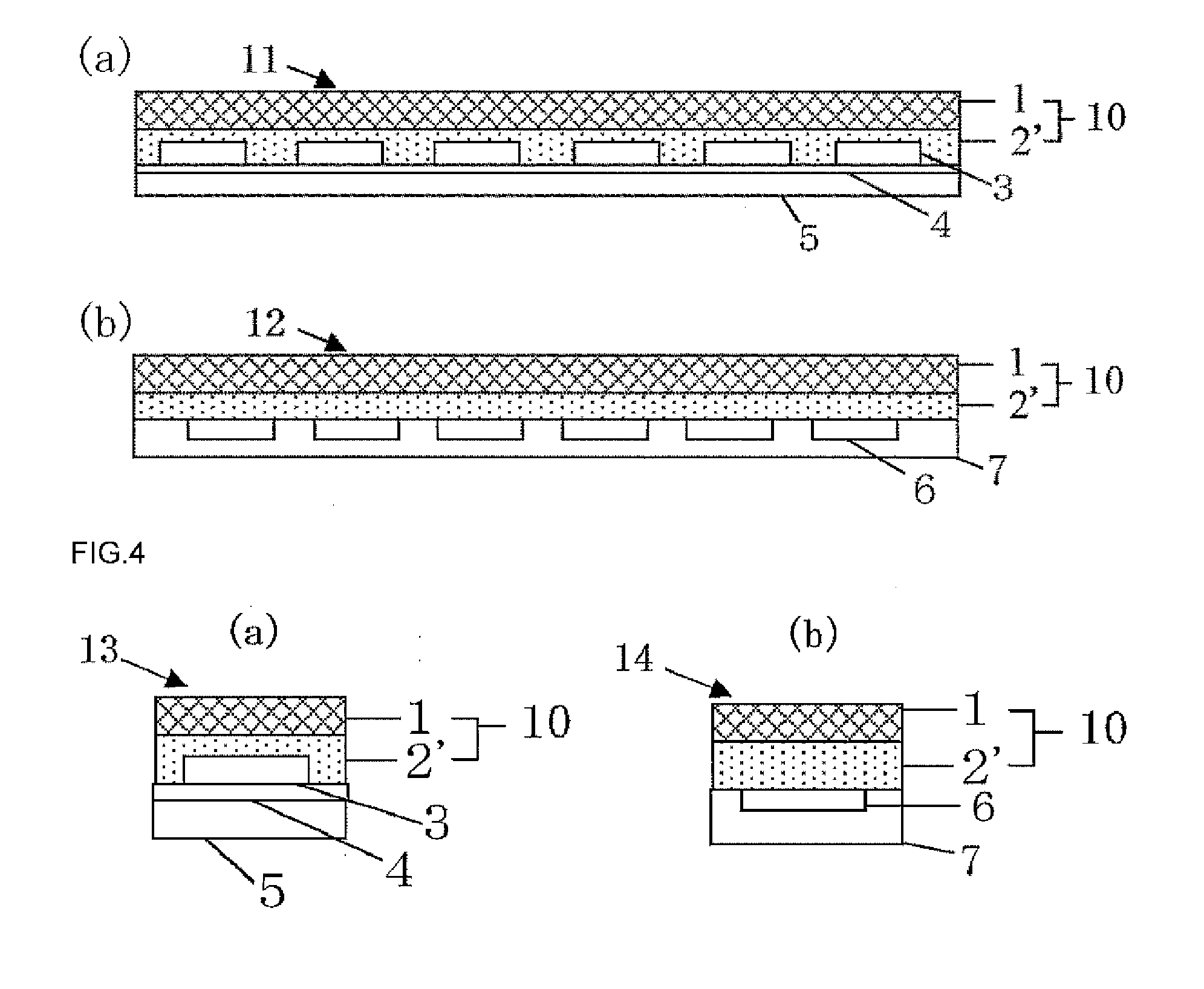
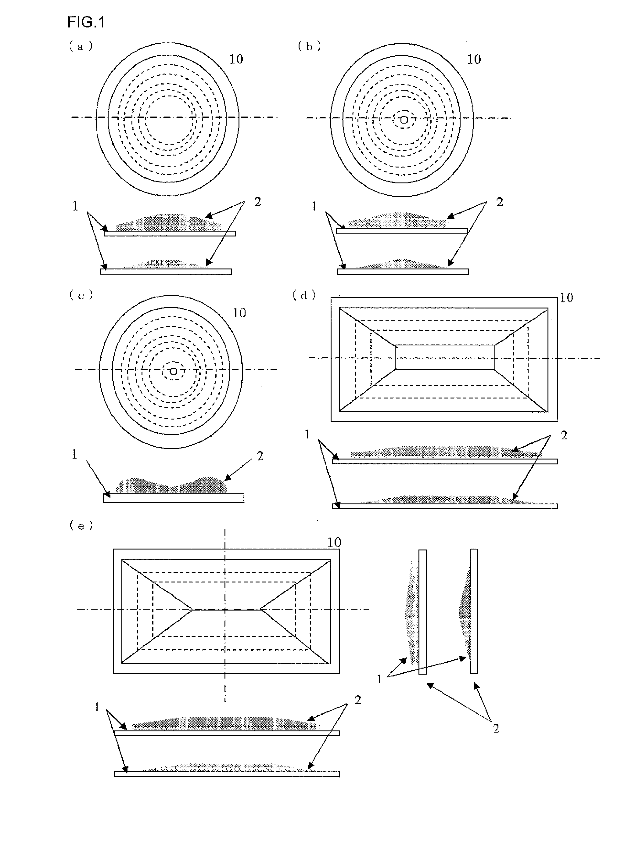
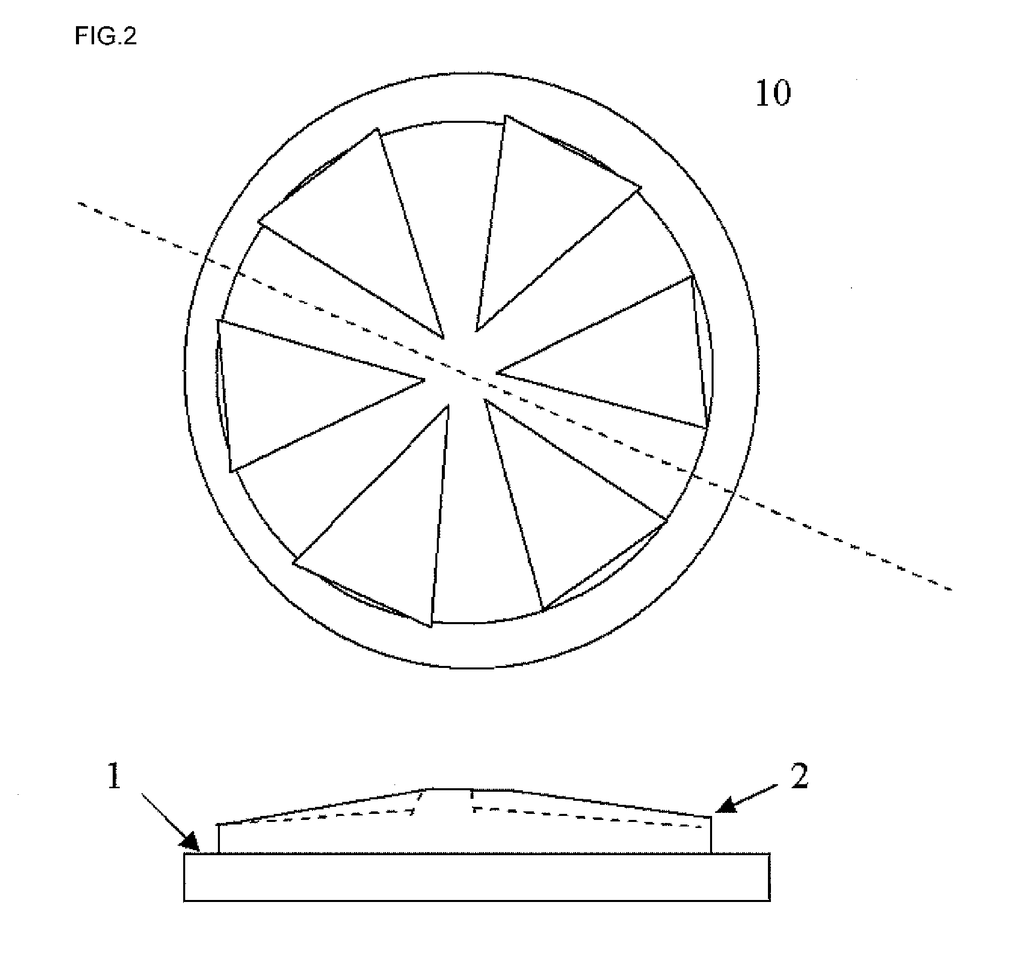
The invention provides an encapsulant equipped with the supporting substrate which is an encapsulant for collectively encapsulating a semiconductor devices mounting surface of a substrate having semiconductor devices mounting thereon or a semiconductor devices forming surface of a wafer having semiconductor devices forming thereon, and the encapsulant equipped with the supporting substrate comprises a supporting substrate having a difference of a linear expansion coefficient from that of the substrate or the wafer of 5 ppm or less and a thermosetting resin layer being laminated, wherein the thermosetting resin layer has a shape having a height difference to a thickness direction.

Description

BACKGROUND OF THE INVENTION[0001]1. Field of the Invention[0002]The present invention relates to an encapsulant equipped with a supporting substrate, an encapsulated substrate having semiconductor devices mounting thereon or an encapsulated wafer having semiconductor devices forming thereon using the encapsulant equipped with the supporting substrate, a semiconductor apparatus manufactured by these and a method for manufacturing the same.[0003]2. Description of the Related Art[0004]A method for encapsulating a wafer level or a method for one-surface molding of an organic substrate on which semiconductor devices have been mounted in a matrix state with a thermosetting epoxy resin has heretofore been proposed and investigated (Patent Documents 1 to 3).[0005]When a semiconductor apparatus is manufactured by the above-mentioned method, if a size of a substrate is small, a warp of the substrate after encapsulating can be controlled by adjusting a linear expansion coefficient of the epoxy...

Claims


Application Information

Patent Timeline
Patent Type & Authority Applications(United States)
IPC IPC(8): H01L23/31H01L21/56
CPCH01L23/3114H01L21/561H01L21/565H01L2224/45144H01L2224/48091Y10T428/2495Y10T428/24967
Inventor AKIBA, HIDEKISHIOBARA, TOSHIOSEKIGUCHI, SUSUMUNAKAMURA, TOMOAKI
Owner SHIN ETSU CHEM IND CO LTD
Learn More