Process-compatible sputtering target for forming ferroelectric memory capacitor plates

a technology of ferroelectric memory and capacitor plate, which is applied in the direction of diaphragms, metallic material coating processes, solid-state devices, etc., can solve the problems of inconvenient use, device essentially volatile, and conventional mos capacitors losing their stored charge, so as to achieve a higher density and lower porosity

Inactive Publication Date: 2014-05-29
TEXAS INSTR INC
View PDF4 Cites 7 Cited by
  • Summary
  • Abstract
  • Description
  • Claims
  • Application Information

AI Technical Summary

Benefits of technology

[0016]Embodiments of this invention may be implemented into the formation and use of a sputtering target for a conductive oxide, such as SrRuO3, to be used for the sputter deposition of a conductive film that is to be in contact with a ferroelectric material, such as PZT, in an integrated circuit. The sputtering targe

Problems solved by technology
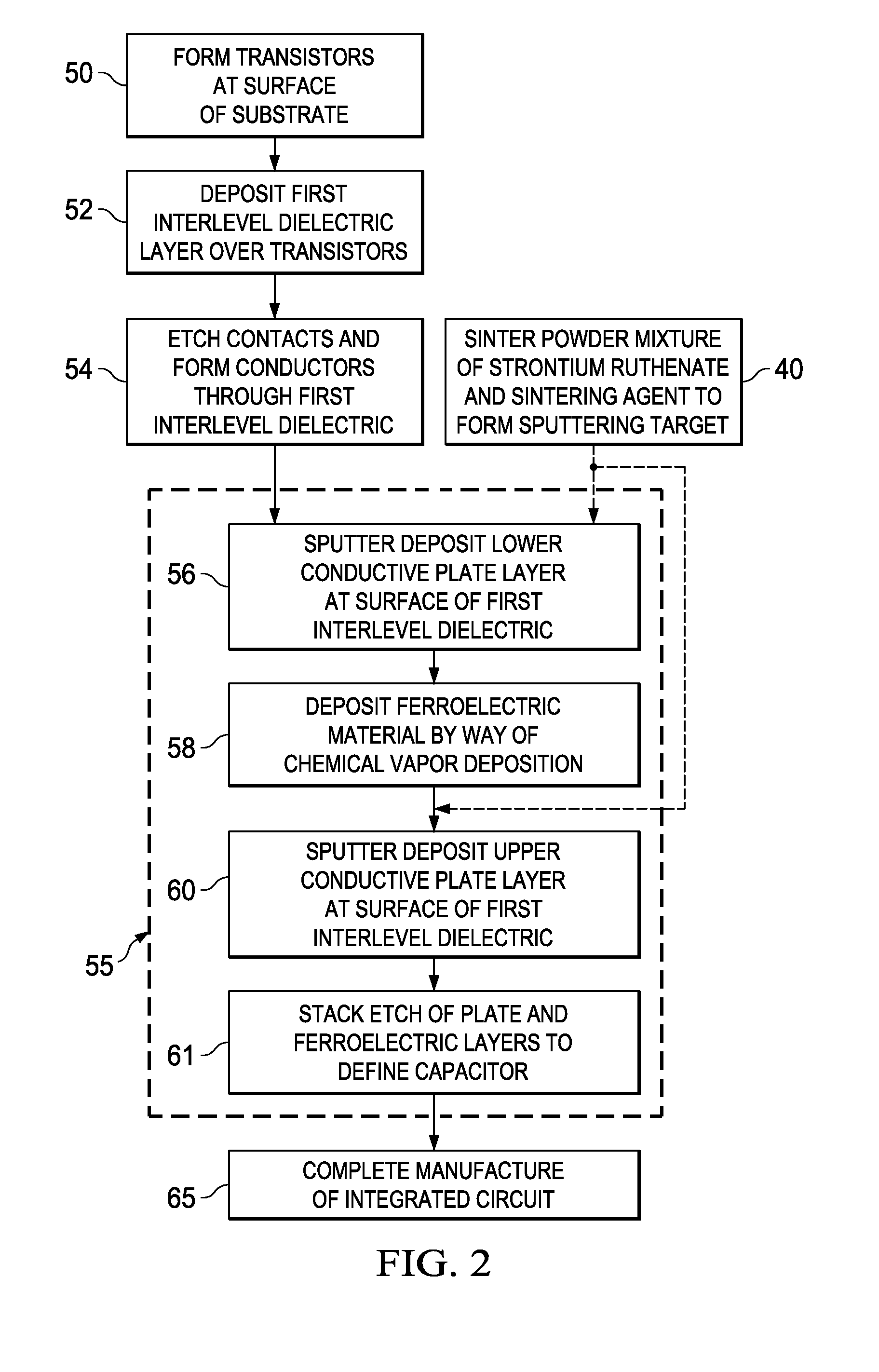
As is fundamental in the art, however, those devices are essentially volatile, in that logic and memory circuits constructed according to these technologies do not retain their data states upon removal of bias power.
In contrast, conventional MOS capacitors lose their stored charge on power-down of the device.
However, these ceramics are generally high temperature materials, and as such are not suitable for melting and cooling into a high density (i.e., low porosity)

Method used


Image

  • Process-compatible sputtering target for forming ferroelectric memory capacitor plates
  • Process-compatible sputtering target for forming ferroelectric memory capacitor plates
  • Process-compatible sputtering target for forming ferroelectric memory capacitor plates

Examples


Embodiment Construction

[0019]This invention will be described in connection with its embodiments, namely as used in the manufacture of semiconductor integrated circuits that include dielectric films of particular ferroelectric or piezoelectric properties, as it is contemplated that this invention is especially beneficial when used in such applications. However, it is contemplated that those skilled in the art having reference to this specification will recognize the benefits and advantages of this invention beyond those applications. Accordingly, it is to be understood that the following description is provided by way of example only, and is not intended to limit the true scope of this invention as claimed.

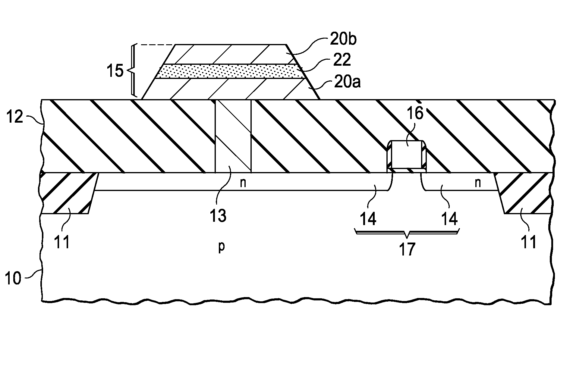
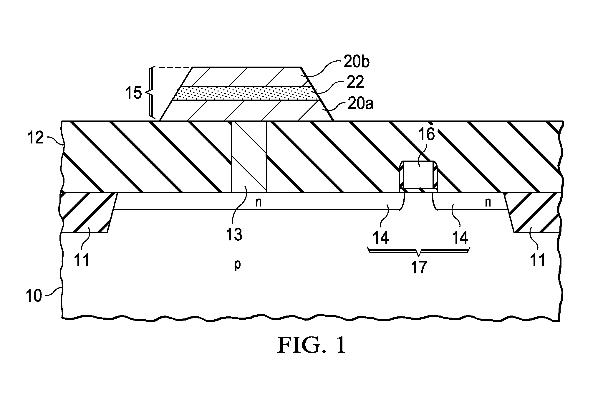
[0020]For purposes of context, FIG. 1 illustrates, in cross-section, a portion of an integrated circuit including a portion of a ferroelectric random access memory (FRAM), as may be constructed using embodiments of the invention. In this example, ferroelectric capacitor 15 and metal-oxide-semiconductor ...


PUM

PropertyMeasurementUnit
Lattice constantaaaaaaaaaa
Densityaaaaaaaaaa
Electrical conductoraaaaaaaaaa

Abstract

A sputtering target for a conductive oxide, such as SrRuO3, to be used for the sputter deposition of a conductive film that is to be in contact with a ferroelectric material in an integrated circuit. The sputtering target is formed by the sintering of a powder mixture of the conductive oxide with a sintering agent of an oxide of one of the constituents of the ferroelectric material. For the example of lead-zirconium-titanate (PZT) as the ferroelectric material, the sintering agent is one or more of a lead oxide, a zirconium oxide, and a titanium oxide. The resulting sputtering target is of higher density and lower porosity, resulting in an improved sputter deposited film that does not include an atomic species beyond those of the ferroelectric material deposited adjacent to that film.

Description

CROSS-REFERENCE TO RELATED APPLICATIONS[0001]This application claims priority, under 35 U.S.C. §119(e), of Provisional Application No. 61 / 729,897, filed Nov. 26, 2012, incorporated herein by this reference.STATEMENT REGARDING FEDERALLY SPONSORED RESEARCH OR DEVELOPMENT[0002]Not applicable.BACKGROUND OF THE INVENTION[0003]This invention is in the field of integrated circuit manufacture. Embodiments of this invention are more specifically directed to the formation of capacitor plates in memory devices such as ferroelectric memories.[0004]Conventional metal-oxide-semiconductor (MOS) and complementary MOS (CMOS) logic and memory devices are prevalent in modern electronic devices and systems, as they provide an excellent combination of fast switching times and low power dissipation, along with their high density and suitability for large-scale integration. As is fundamental in the art, however, those devices are essentially volatile, in that logic and memory circuits constructed accordin...

Claims


Application Information

Patent Timeline
IPC IPC(8): H01L49/02C23C2/00
CPCC23C2/00H01L28/60H01L28/55H10B53/30B22F3/10B22F5/00C22C28/00C22C32/001C22C32/0015C22C32/0031C22C32/0042C23C14/08C23C14/082C23C14/3414H01L21/2855H01L21/32133H01L28/65H01L28/75
Inventor VISOKAY, MARK ROBERTSUMMERFELT, SCOTT ROBERT
Owner TEXAS INSTR INC
Why Eureka
Try Eureka