Direct Growth of Graphene by Molecular Beam Epitaxy for the Formation of Graphene Heterostructures

Inactive Publication Date: 2014-07-31
UNIVERSITY OF NORTH TEXAS
View PDF12 Cites 4 Cited by
  • Summary
  • Abstract
  • Description
  • Claims
  • Application Information

AI Technical Summary

Benefits of technology

This patent presents evidence of the formation of continuous layers of graphene on thin films of Co3O4 and Auger and XPS data confirm the absence of a band gap in the graphene layers. The growth of graphene on Co3O4 is compared to the growth on MgO, which suggests that the graphene layers are separated from the substrate due to strong interactions with the substrate. The results also show that the use of MBE at high temperature does not limit the number of graphene layers that can be formed. Structural similarity between Co3O4 and magnetoelectric Cr2O3 implies potential spintronic applications.

Problems solved by technology

The physical transfer approach poses significant problems for device integration, including the formation of nanoscale inhomogeneities [9,10], and SiO2 phonon-induced limits on graphene carrier mobilities [11].
The integration of SiC with Si also poses significant issues.

Method used


Image

  • Direct Growth of Graphene by Molecular Beam Epitaxy for the Formation of Graphene Heterostructures
  • Direct Growth of Graphene by Molecular Beam Epitaxy for the Formation of Graphene Heterostructures
  • Direct Growth of Graphene by Molecular Beam Epitaxy for the Formation of Graphene Heterostructures

Examples


Embodiment Construction

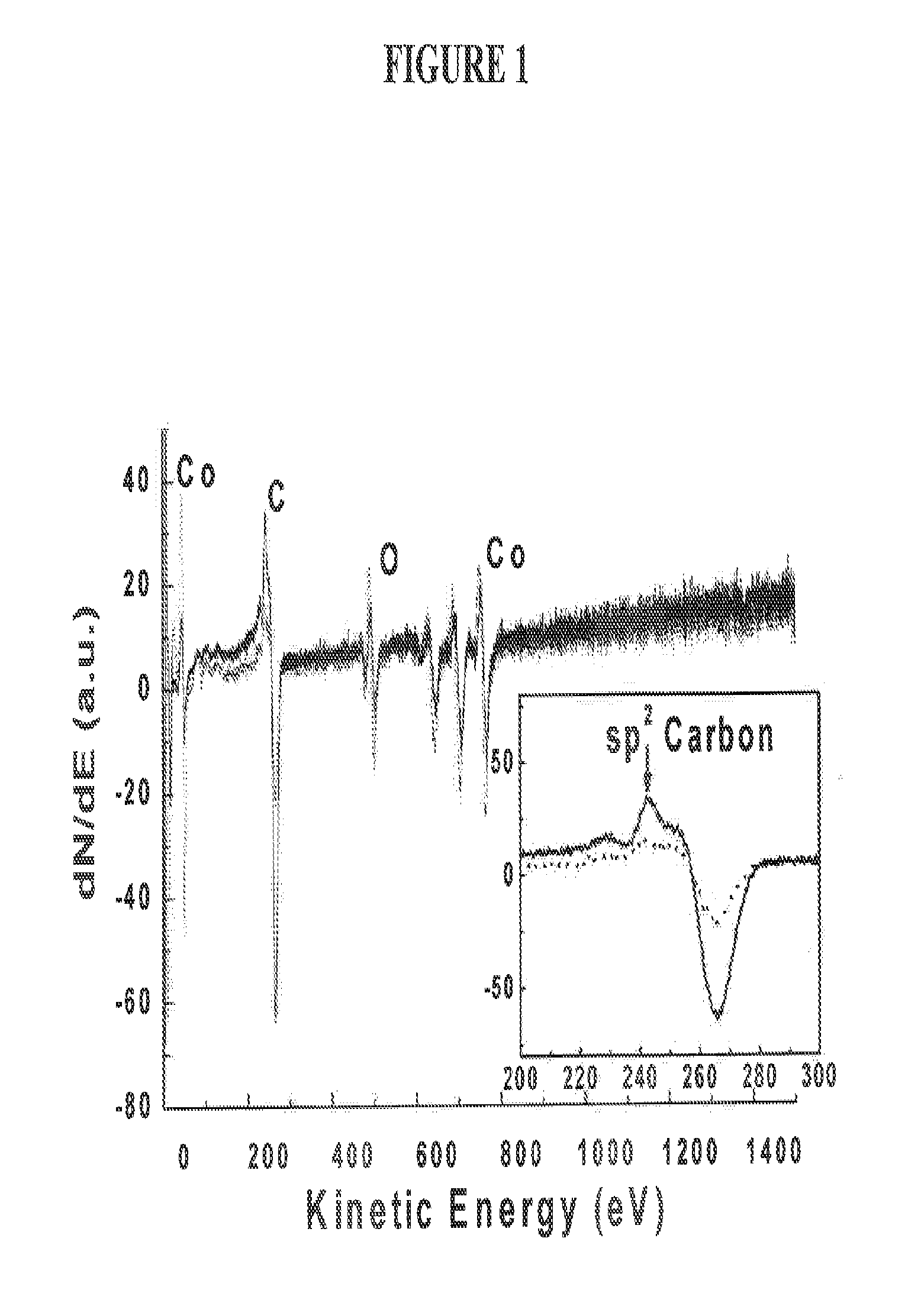
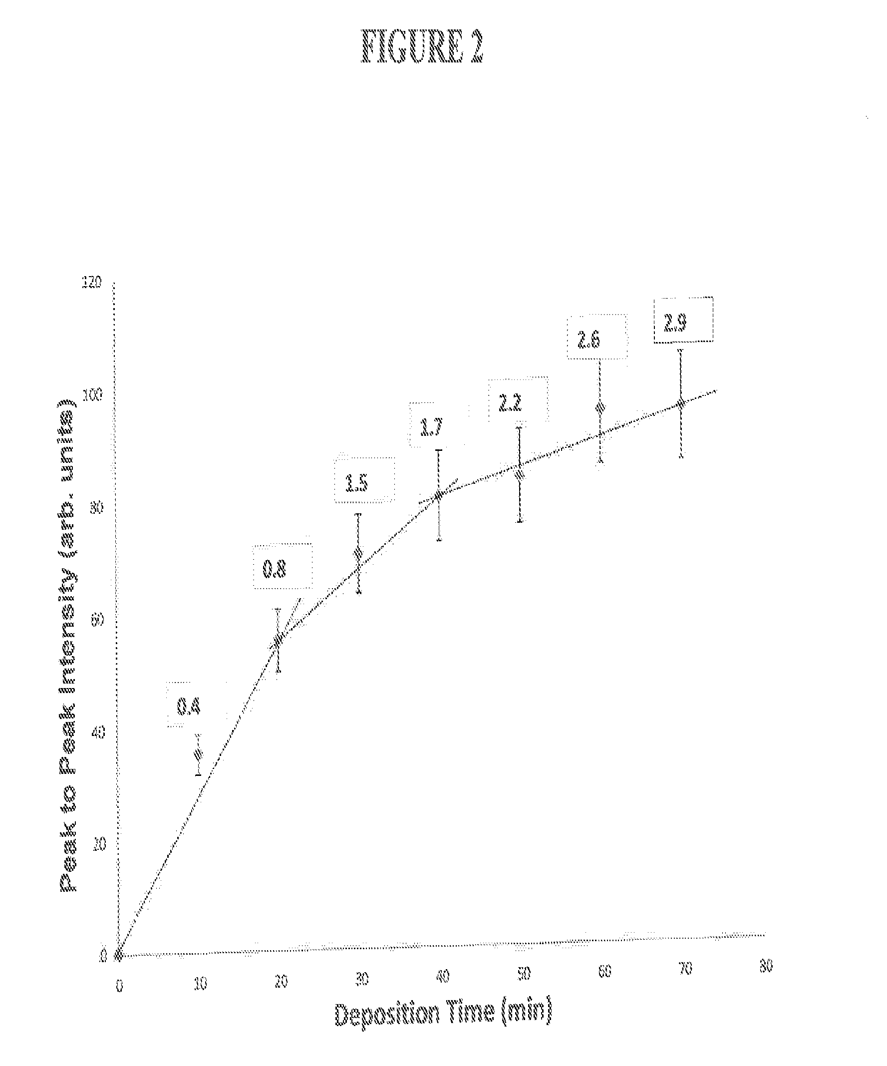
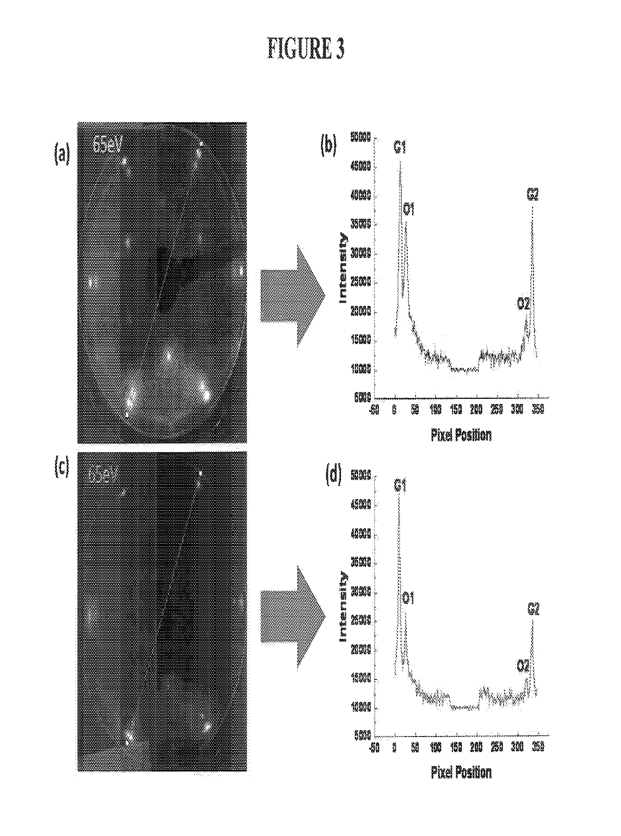
[0015]AES and LEED studies were carried out in a system described previously [17], but equipped with a commercially available multisource cell for electron beam-induced evaporation of Co and carbon from Co rod and graphite rod targets. The evaporator / sample distance was ˜9 cm. Co films ˜50 Å thick were deposited from a Co rod at 750 K onto 1 cm2 Al2O3(0001) substrates. The base pressure in the chamber was ˜3×10⁻¹⁰ Torr, which increased during deposition to ˜5×10⁻⁹ Torr. Pressures remain below 1×10⁻⁸ throughout. Films were subsequently annealed in ultrahigh vacuum (UHV) to 1000 K, which allowed oxygen—dissolved in the Co film during deposition—to segregate to the surface and form a surface oxide film ˜3 ML thick, as determined by XPS (see below). Graphene films were deposited from a graphite rod with the sample at 1000 K. AES and LEED data were acquired after each deposition of carbon. XPS studies were carried out in a separate UHV chamber described previously [18], using a non-monoc...


PUM


Abstract

Growth of single- and few-layer macroscopically continuous graphene films on Co3O4(111) by molecular beam epitaxy (MBE) has been characterized using low energy electron diffraction (LEED), Auger electron spectroscopy (AES) and x-ray photoelectron spectroscopy (XPS). MBE of Co on sapphire(0001) at 750 K followed by annealing in UHV (1000 K) results in ˜3 monolayers (ML) of Co3O4(111) due to O segregation from the bulk. Subsequent MBE of C at 1000 K from a graphite source yields a graphene LEED pattern incommensurate with that of the oxide, indicating graphene electronically decoupled from the oxide, as well as a sp2 C(KVV) Auger lineshape, and π→π* C(1s) XPS satellite. The data strongly suggest the ability to grow graphene on other structurally similar magnetic / magnetoelecric oxides, such as Cr2O3(111) / Si for spintronic applications.

Description

PRIORITY DATA AND INCORPORATION BY REFERENCE[0001]This application is a national stage application from PCT Patent Application Serial No. PCT / US12 / 46621, filed Jul. 13, 2012, which claims benefit of priority to U.S. Provisional Patent Application Ser. No. 61 / 507,722 filed Jul. 14, 2011, and U.S. Provisional Patent Application Ser. No. 61 / 521,600 filed Aug. 9, 2011 which is incorporated by reference in its entirety.BACKGROUND OF THE INVENTION[0002]1. Field of the Invention[0003]This application is directed to the direct growth of graphene layers on heterostructures and dielectric substrate surfaces for the purposes of forming logic devices and interconnects. This work was supported in part by Semiconductor Research Corporation, Task ID 2123.001.[0004]2. Related Art[0005]This case is generally related to the deposition of graphene on MgO surfaces, reported in U.S. patent application Ser. No. 12 / 980,767 and graphene on BN surfaces reported in U.S. Pat. No. 8,158,200. Both of these docu...

Claims


Application Information

Patent Timeline
IPC IPC(8): C30B23/06H01L43/10C01B31/04
CPCH01L29/1606C01B31/0461B82Y30/00H01L21/02381H01L21/0242H01L21/02433H01L21/02488H01L21/02516H01L21/02527H01L21/02631C01B31/0438C30B23/066H01L43/10B82Y40/00C01B32/182C01B32/188Y10T428/30H10N50/85
Inventor KELBER, JEFFRY
Owner UNIVERSITY OF NORTH TEXAS
Why Eureka
Try Eureka