Semiconductor device

a technology of semiconductor devices and semiconductors, applied in the direction of semiconductor devices, basic electric elements, electrical appliances, etc., can solve the problems of reducing the withstand voltage between the source electrode se and the drain electrode de with the increase of leakage current, affecting the performance of the power fet, so as to improve the performance of the semiconductor device

Active Publication Date: 2014-09-18
RENESAS ELECTRONICS CORP
View PDF7 Cites 24 Cited by
  • Summary
  • Abstract
  • Description
  • Claims
  • Application Information

AI Technical Summary

Benefits of technology

[0010]According to the semiconductor device of an embodiment, it is possible to enhance the performance of the semiconductor device.

Problems solved by technology

Therefore, the leakage current from the channel layer CH via the buffer layer BUF cannot be ignored, and as a result, the withstand voltage between the source electrode SE and the drain electrode DE decreases with the increase in the leakage current.
This is because, in the nitride semiconductor layer, since the band gap is large, an energy difference between the acceptor level of the acceptors and the upper end of a valence band is large, and as a result, electrons are difficult to be excited from the valence band to the acceptor level.
That is, when the channel layer CH including gallium nitride (GaN) is directly formed over the semiconductor substrate 1S including silicon, many crystal defects are formed in the channel layer CH, and thus the performance of the power FET degrades.
When the number of such deep levels increases in the power FET, there is increased a risk that a current variation such as a so-called current collapse or a drift variation is caused.
However, in this configuration, the band gap of the p-type semiconductor layer is still small.
Therefore, even if the p-type semiconductor layer is formed between the buffer layer BUF and the channel layer CH, the band gap is smaller than that of the channel layer CH, and thus the leakage current cannot be suppressed.
That is, in this configuration, the p-type semiconductor layer does not sufficiently function as a barrier to the leakage current, and thus it is difficult to sufficiently reduce the leakage current, from the channel layer CH, via the p-type semiconductor layer and the buffer layer BUF.
Therefore, in the configuration in which the p-type semiconductor layer including the nitride semiconductor layer LBL having a small band gap is simply formed between the buffer layer BUF and the channel layer CH, the leakage current between the source electrode SE and the drain electrode DE via the buffer layer BUF is not sufficiently suppressed, and thus it is difficult to enhance the withstand voltage between the source electrode SE and the drain electrode DE.
Moreover, magnesium (Mg) is purposely not added to the nitride semiconductor layer HBL having a low activation rate and including an AlGaN layer, and thus deep levels are difficult to be generated and the current collapse can be suppressed.
However, when the film thickness of the InGaN layer is too thick, there is a risk that a part of the conduction band of the InGaN layer falls below the Fermi level at an interface between the InGaN layer and the AlGaN layer that form the superlattice layer PSL due to the slope of the band based on the piezoelectric polarization and electrons are accumulated.
In this case, there is a risk that positive holes caused by the acceptors are offset, and thus the film thickness of the InGaN layer is required to be appropriately adjusted within a range of the critical film thickness.
However, when the composition ratio of aluminum in the AlGaN layer is too large, there is a risk that a part of the conduction band of the AlGaN layer falls below the Fermi level and electrons are accumulated, at an interface between the InGaN layer and the AlGaN layer which form the superlattice layer PSL due to the slope of the band based on the piezoelectric polarization.
However, electrons travel in the channel layer CH, and thus when a large amount of conductive impurities are added, there is a risk that the mobility of the electrons decreases because of Coulomb scattering.
However, in the ridge structure, the widths of the p-type clad layer PCL and the p-type contact layer PCNT are small, and thus the element resistance inevitably becomes large and it can also be said that the ridge structure is a structure in which low voltage operation is difficult.
In this case, in the semiconductor laser, there is a risk that a current fluctuation occurs on the basis of a large number of deep levels formed in the p-type clad layer PCL.
Therefore, there is concern that the current fluctuation significantly affects the direct modulation of the semiconductor laser.

Method used


Image

  • Semiconductor device
  • Semiconductor device
  • Semiconductor device

Examples


first embodiment

Description of Related Art

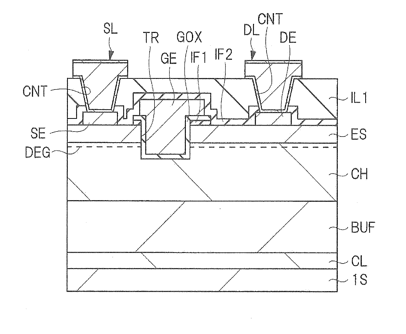
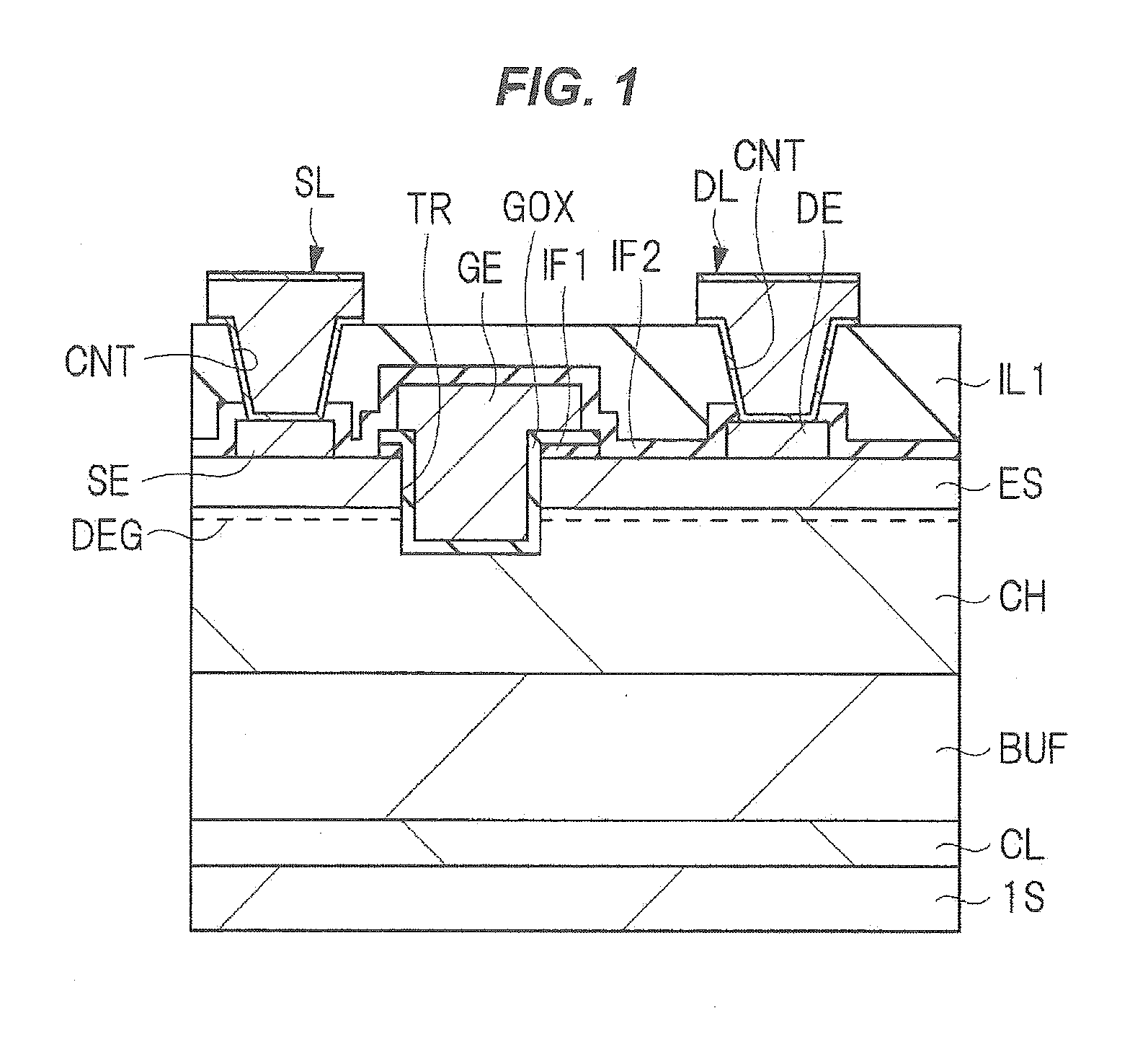
[0034]FIG. 1 is a cross-sectional view showing a configuration example of a semiconductor device according to a related art 1. In the related art 1, a power FET (Field Effect Transistor) including a high electron mobility transistor will be described as an example of the semiconductor device.

[0035]As shown in FIG. 1, in the power FET of the related art 1, a buffer layer BUF including, for example, an Al0.07Ga0.93N layer is formed over a semiconductor substrate 1S including, for example, silicon, via a nucleation layer CL including, for example, an AlN layer (nitride aluminum layer). In addition, a high-electron-mobility layer (channel layer) CH including, for example, a GaN layer is formed over the buffer layer BUF and an electron supply layer ES including, for example, an AlGaN layer (Al0.22Ga0.78N) is formed over the channel layer CH.

[0036]Next, as shown in FIG. 1, in the power FET of the related art 1, there is formed an insulating film IF1 including, fo...

second embodiment

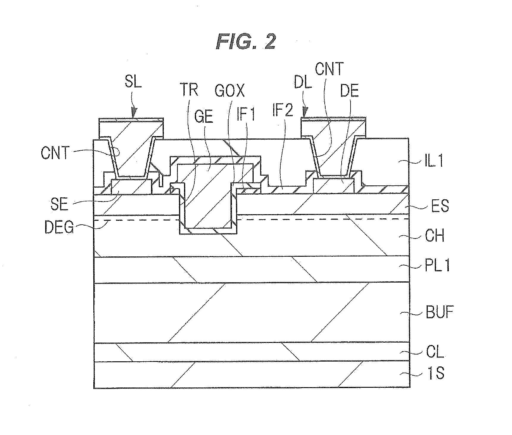
[0130]In a power FET including a high electron mobility transistor according to the present second embodiment, only the structure of the gate electrode is different from that of the power FET according to the first embodiment. In FIG. 3 showing the power FET according to the first embodiment, the trench TR is formed, and the gate insulating film GOX covering the inner wall of the trench TR and the gate electrode GE in contact with the gate insulating film GOX are formed.

[0131]On the other hand, FIG. 15 is a cross-sectional view showing a configuration of the power FET according to the Present second embodiment. In the present second embodiment, as shown in FIG. 15, a p-type cap layer PCP is formed in contact with the electron supply layer ES and the gate electrode GE is formed over the p-type cap layer PCP. At this time, it is desirable that the p-type cap layer PCP and the gate electrode GE are schottky-coupled to electrons. In addition, a gate insulating film (not shown in the dra...

third embodiment

[0139]In the first embodiment and the second embodiment, a power FET including a high electron mobility transistor has been described as an application example of the technical idea, and in the present third embodiment, a semiconductor laser will be described as an application example of the technical idea.

[0140]

For example, a semiconductor laser is used for recording and reproduction of an optical disk. In recent years, a short wavelength semiconductor laser has been often used for recording and reproduction of an optical disk as capacities and densities of optical disks increase. That is, as semiconductor lasers used for recording of an optical disk, the demand for blue-violet semiconductor lasers whose wavelength is shorter than that of red semiconductor lasers is increasing.

[0141]A semiconductor laser emits light corresponding to the magnitude of the band gap of the semiconductor material, and thus it is necessary to use a semiconductor material having a large band gap in order ...


PUM

PropertyMeasurementUnit
threshold voltageaaaaaaaaaa
thicknessaaaaaaaaaa

Abstract

To improve performance of a semiconductor device. For example, on the assumption that a superlattice layer is inserted between a buffer layer and a channel layer, a concentration of acceptors introduced into nitride semiconductor layers forming a part of the superlattice layer is higher than a concentration of acceptors introduced into nitride semiconductor layers forming the other part of the superlattice layer. That is, the concentration of acceptors introduced into the nitride semiconductor layers having a small band gap is higher than the concentration of acceptors introduced into the nitride semiconductor layers having a large band gap.

Description

CROSS-REFERENCE TO RELATED APPLICATION[0001]The disclosure of Japanese Patent Application No. 2013-051047 filed on Mar. 13, 2013 including the specification, drawings and abstract is incorporated herein by reference in its entirety.BACKGROUND[0002]The present invention relates to a semiconductor device, for example, relates to an effective technique to be applied to a semiconductor device using nitride semiconductor layers.[0003]Japanese Patent No. 3960957 (Patent Document 1) describes a technique for forming a buffer layer from a laminated structure of a first layer formed of a GaN layer that is a nitride semiconductor layer and a second layer formed of an AlGaN layer that is a nitride semiconductor layer and having a band larger than that of the first layer. In this technique, magnesium (Mg) that is an acceptor is introduced into both the first layer and the second layer and the addition amount of the magnesium introduced into the first layer and the addition amount of the magnesi...

Claims


Application Information

Patent Timeline
Patent Type & Authority Applications(United States)
IPC IPC(8): H01L29/778
CPCH01L29/7783H01L29/66462H01L29/155H01L29/2003H01L29/7787
Inventor NAKAYAMA, TATSUOMIYAMOTO, HIRONOBUOKAMOTO, YASUHIRONEGA, RYOHEIKANAZAWA, MASAAKIINOUE, TAKASHI
Owner RENESAS ELECTRONICS CORP
Why Eureka
Try Eureka