Conductive pattern formation method and composition for forming conductive pattern via photo irradiation or microwave heating
- Summary
- Abstract
- Description
- Claims
- Application Information
AI Technical Summary
Benefits of technology
Problems solved by technology
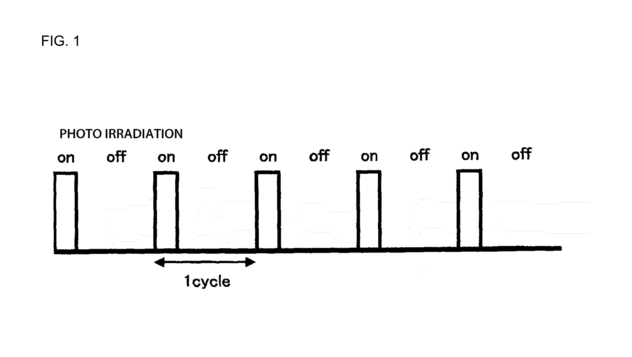
Method used
Image

Examples
example 1
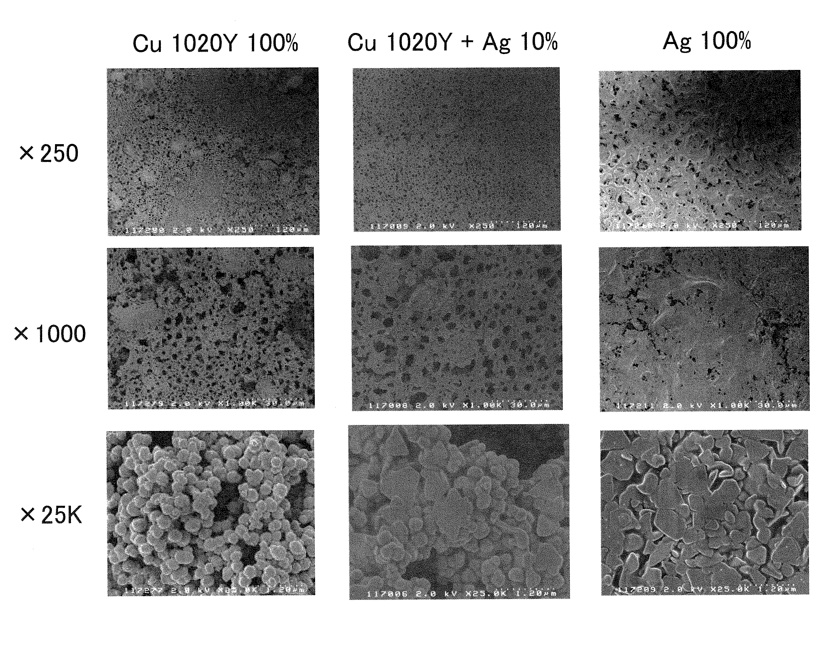
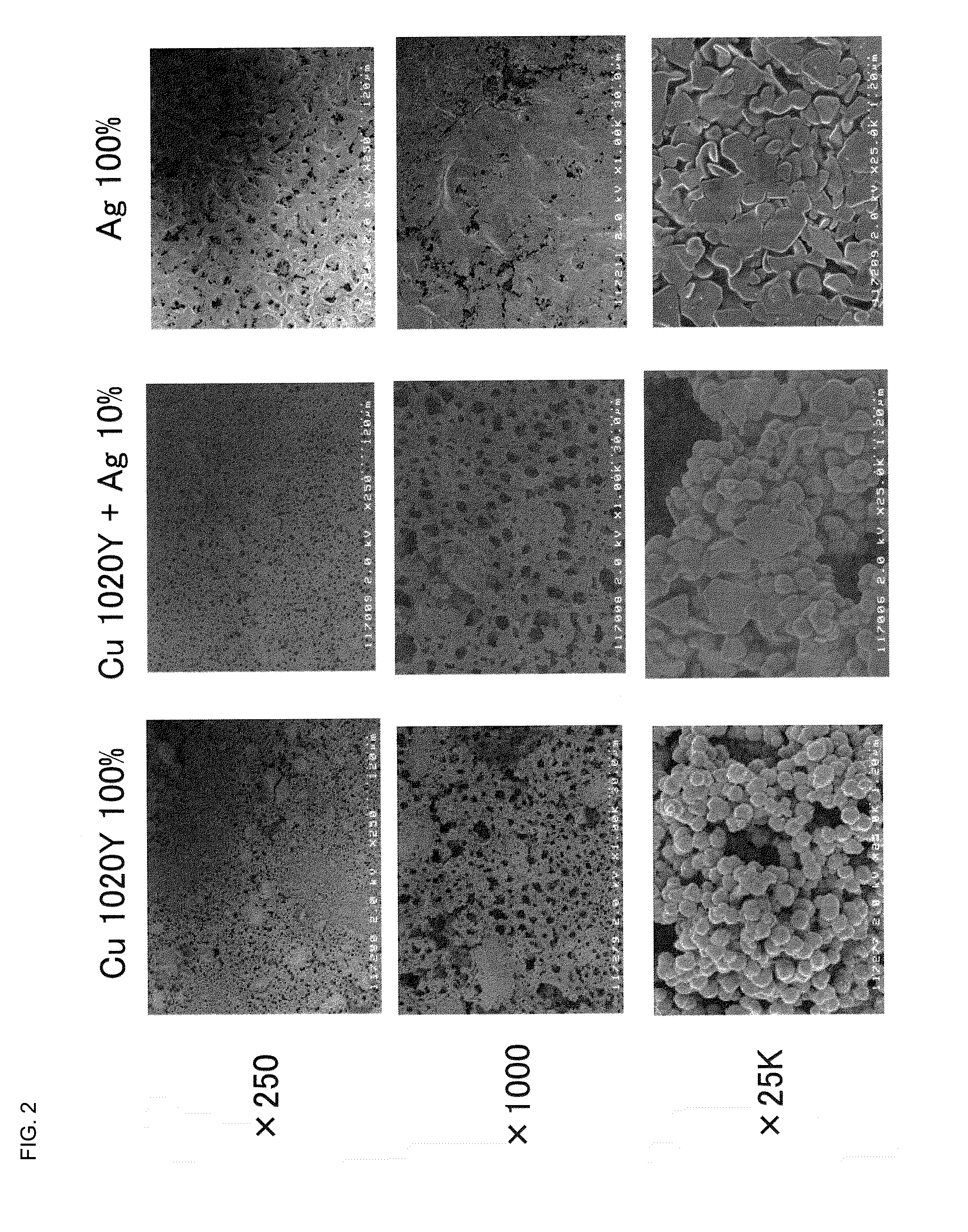
[0051]Polyvinylpyrrolidone (made by Nippon Shokubai Co., Ltd.) as a binder was dissolved into a mixed aqueous solution of ethyleneglycol and glycerin (a reagent made by Kanto Chemical Co., Inc.) as a reducing agent to prepare a binder solution of 40 mass %. A mass ratio of ethyleneglycol and glycerin and water in the mixed aqueous solution is 70:15:15. Then, 1.5 g of this solution was mixed with 0.5 g of the above mentioned mixed aqueous solution, into which 5.4 g of copper powder 1050Y (spherical, D50=716 nm) made by Mitsui Mining and Smelting Co., Ltd. and 0.6 g of N300 as silver particles (flat (thickness: 30 nm), D50=470 nm) made by Tokusen Co., Ltd. were mixed (copper particles:silver particles=90:10), and well mixed using Planetary Centrifugal Vacuum Mixer “Thinky Mixer” (AWATORI RENTAROU) ARV-310 (manufactured by Thinky Corporation) to prepare a paste for printing (composition for forming a conductive pattern).
[0052]The obtained paste was printed on a polyimide film (Kapton 1...
example 2
[0053]5.4 g of copper powder 1100Y made by Mitsui Mining & Smelting Co., Ltd. (spherical, D50=1110 nm) and 0.6 g of N300 as silver particles (flat (thickness: 30 nm), D50=470 nm) made by Tokusen Co., Ltd. were used to prepare a paste for printing in the same manner as that in Example 1. The obtained paste was printed in a pattern in the same manner as that in Example 1, and subjected to photo irradiation. The thickness of the conductive pattern formed was 23 μm.
example 3
[0054]5.4 g of copper powder 1400Y made by Mitsui Mining & Smelting Co., Ltd. (spherical, D50=5700 nm) and 0.6 g of N300 as silver particles (flat (thickness: 30 nm), D50=470 nm) made by Tokusen Co., Ltd. were used to prepare a paste for printing in the same manner as that in Example 1. The obtained paste was printed in a pattern in the same manner as that in Example 1, and subjected to photo irradiation. The thickness of the conductive pattern formed was 26 μm.
PUM
| Property | Measurement | Unit |
|---|---|---|
| Thickness | aaaaa | aaaaa |
| Thickness | aaaaa | aaaaa |
| Nanoscale particle size | aaaaa | aaaaa |
Abstract
Description
Claims
Application Information
PatSnap Eureka turns technology decisions into work you can execute. Powered by our Innovation Knowledge Graph, it runs expert workflows across engineering, life sciences, materials and intellectual property. Get your review-ready output in minutes.


