Capacitive micro-machined transducer and method of manufacturing the same

a micro-machined transducer and capacitive technology, applied in the direction of mechanical vibration separation, generator/motor, coating, etc., can solve the problems of limited cmut performance, inconvenient operation, and inability to charge, so as to improve the output pressure, improve the performance, and reduce the operating voltage

Active Publication Date: 2014-12-25
KONINKLJIJKE PHILIPS NV
View PDF8 Cites 11 Cited by
  • Summary
  • Abstract
  • Description
  • Claims
  • Application Information

AI Technical Summary

Benefits of technology

[0005]It is an object of the present invention to provide an improved capacitive micro-machined transducer (in particular CMUT), in particular with improved performance (e.g. lowering the operating voltage and / or increasing the output pressure) and / or easier to manufacture. It is a further object of the present invention to provide an improved method of manufacturing such capacitive micro-machined transducer (in particular CMUT).

Problems solved by technology

However, charging is a known disadvantage of capacitive micro-machined ultrasound transducer.
However, an ONO dielectric layer has its limitations and can be deposited only at relative thick layers (e.g. about 250 nm using PECVD) and a low dielectric constant, as the dielectric constant of nitride is about 5 to 7.
Thus, the performance of the CMUT is limited by a minimum thickness of the ONO dielectric layer, the electrical breakdown voltage and its dielectric constant.
A particular problem with such a CMUT device can be that the operating voltage is rather high and the output pressure relatively low.

Method used


Image

  • Capacitive micro-machined transducer and method of manufacturing the same
  • Capacitive micro-machined transducer and method of manufacturing the same
  • Capacitive micro-machined transducer and method of manufacturing the same

Examples


first embodiment

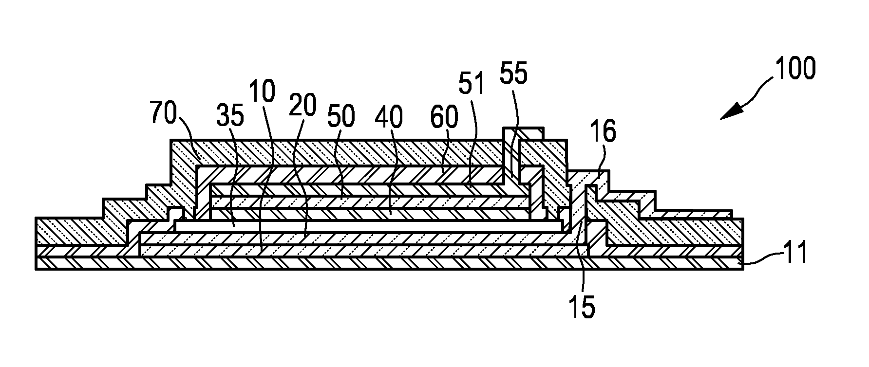
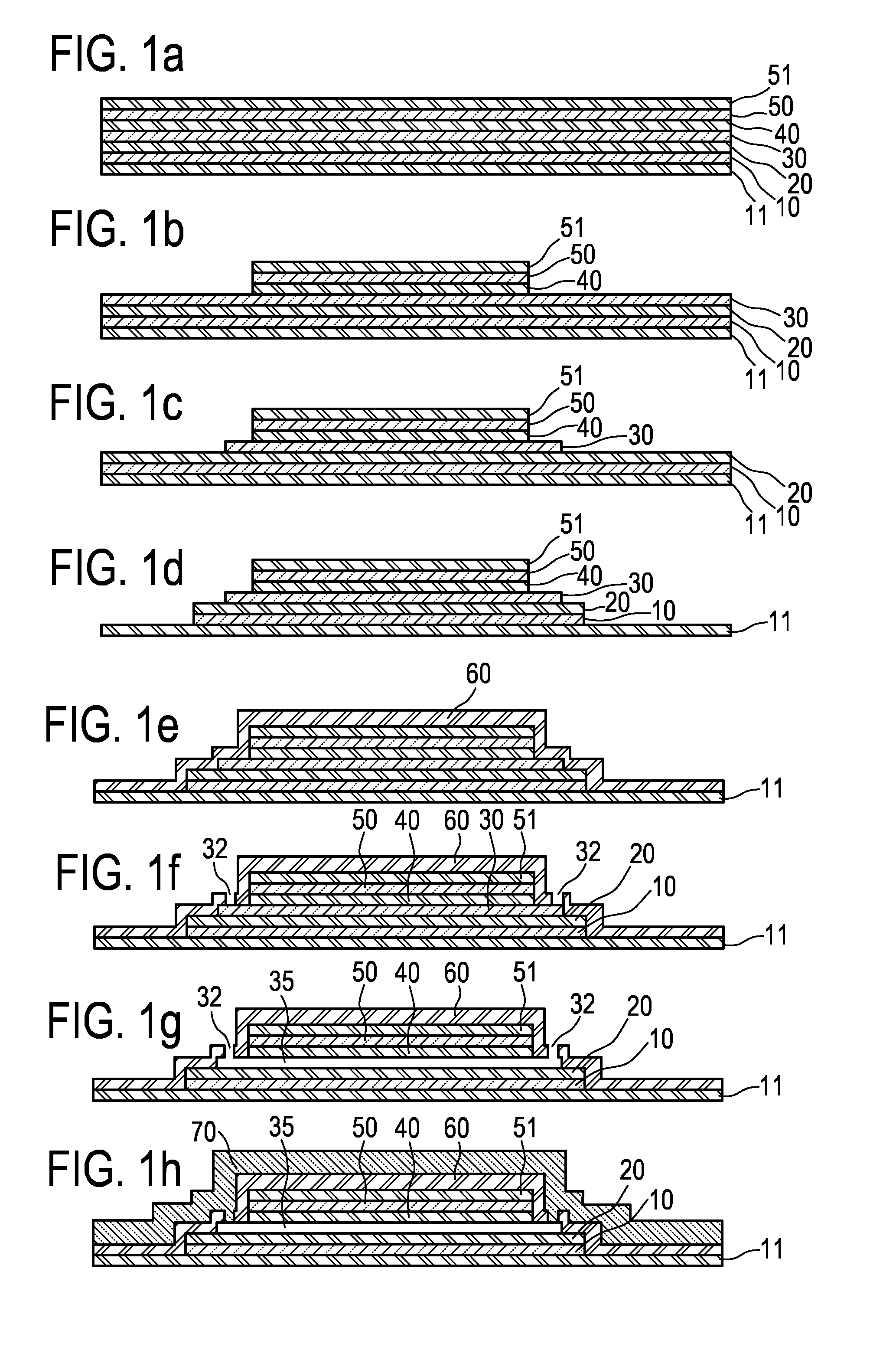
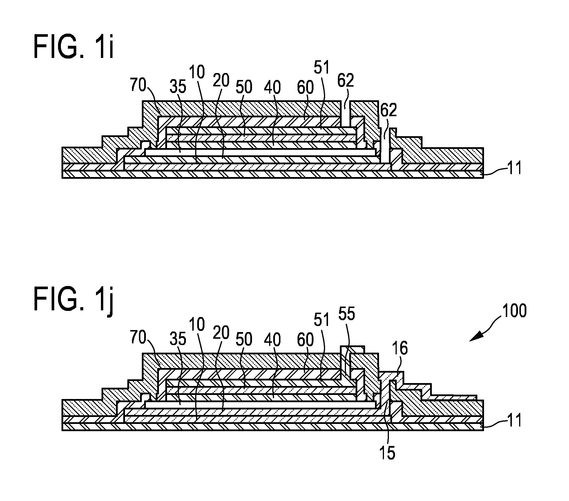
[0038]FIG. 1a-j show a method of manufacturing a CMUT 100 according to a In particular, FIG. 1b-j show a schematic top to bottom process flow, after all functional CMUT layers have been deposited in one process sequence (see FIG. 1a) by using Atomic Layer Deposition (ALD).

[0039]The method starts with the process sequence of using ALD (see FIG. 1a). First, a first electrode layer 10 is deposited on a substrate (not shown) or dielectric layer 11. In the embodiment shown in FIG. 1a, the dielectric layer 11 is provided or deposited between the substrate and the first electrode layer 10. Dielectric layer 11 is in this case the first layer on the substrate. In this case, the dielectric layer can for example be made of (Silicon) Oxide or (Silicon) Nitride, in particular when processing on an ASIC, where often a planarization step is used to create a smooth surface. However, dielectric layer 11 could also be omitted. Then, a first dielectric film 20 is deposited on the first electrode laye...

second embodiment

[0046]FIG. 2a-j show a manufacturing method of a CMUT according to a In this embodiment, a substrate 1 comprises an ASIC 2 integrated therein and a conductive via 15 in the substrate. Alternatively, the ASIC 2 could also be attached to the substrate 1. The method starts with depositing a first electrode layer 10 on the substrate 1. Then, a first dielectric film 20 is deposited on the first electrode layer 10, and a sacrificial layer 30 is deposited on the first dielectric film 20. The sacrificial layer 30 is removable for forming a cavity of the transducer later on. Subsequently, a second dielectric film 40 is deposited on the sacrificial layer 30. Then, a second electrode layer 50 is deposited on the second dielectric film 40. Each of these depositing steps is performed by Atomic Layer Deposition (ALD). In this way a stack of alternating layers of a dielectric material and a conductive material are provided (see FIG. 2b). Thus, all CMUT functional layers (AL-ALD CMUT) are deposite...

third embodiment

[0053]Also in this third embodiment, a substrate 1 comprises an ASIC 2 integrated therein and a conductive via 15 in the substrate 1. The method starts with depositing a first electrode layer 10 on the substrate 1. Then, a first dielectric film 20 is deposited on the first electrode layer 10, and a sacrificial layer 30 is deposited on the first dielectric film 20. The sacrificial layer 30 is removable for forming a cavity of the transducer later on. Subsequently, a second dielectric film 40 is deposited on the sacrificial layer 30. Then, a second electrode layer 50 is deposited on the second dielectric film 40. Each of these depositing steps is performed by Atomic Layer Deposition (ALD). In this way a stack of alternating layers of a dielectric material and a conductive material are provided (see FIG. 3a). Thus, all CMUT functional layers (AL-ALD CMUT) are deposited in one single process sequence.

[0054]The method further comprises patterning all of the deposited layers and films 10,...


PUM

PropertyMeasurementUnit
dielectric constantaaaaaaaaaa
thicknessaaaaaaaaaa
frequenciesaaaaaaaaaa

Abstract

The present invention relates to a method of manufacturing a capacitive micro-machined transducer (100), in particular a CMUT, the method comprising depositing a first electrode layer (10) on a substrate (1), depositing a first dielectric film (20) on the first electrode layer (10), depositing a sacrificial layer (30) on the first dielectric film (20), the sacrificial layer (30) being removable for forming a cavity (35) of the transducer, depositing a second dielectric film (40) on the sacrificial layer (30), and depositing a second electrode layer (50) on the second dielectric film (40), wherein the first dielectric film (20) and/or the second dielectric film (40) comprises a first layer comprising an oxide, a second layer comprising a high-k material, and a third layer comprising an oxide, and wherein the depositing steps are performed by Atomic Layer Deposition. The present invention further relates to a capacitive micro-machined transducer (100), in particular a CMUT, manufactured by such method.

Description

FIELD OF THE INVENTION[0001]The present invention relates to a method of manufacturing a capacitive micro-machined transducer, in particular a capacitive micro-machined ultrasound transducer (CMUT) for transmitting and / or receiving ultrasound waves. The present invention further relates to a capacitive micro-machined transducer, in particular a capacitive micro-machined ultrasound transducer (CMUT) for transmitting and / or receiving ultrasound.BACKGROUND OF THE INVENTION[0002]The heart of any ultrasound (imaging) system is the transducer which converts electrical energy in acoustic energy and back. Traditionally, these transducers are made from piezoelectric crystals arranged in linear (1-D) transducer arrays, and operating at frequencies up to 10 MHz. However, the trend towards matrix (2-D) transducer arrays and the drive towards miniaturization to integrate ultrasound (imaging) functionality into catheters and guide wires has resulted in the development of so-called capacitive micr...

Claims


Application Information

Patent Timeline
Patent Type & Authority Applications(United States)
IPC IPC(8): B06B1/02B81C1/00B81B3/00
CPCB06B1/0292B81C1/00373B81B3/00B81C1/00158B81B2203/0127B06B1/02H02N1/006H02N1/08
Inventor DIRKSEN, PETERMAUCZOK, RUEDIGERKARAKAYA, KORAYKLOOTWIJK, JOHAN HENDRIKMARCELIS, BOUTMULDER, MARCEL
Owner KONINKLJIJKE PHILIPS NV
Why Eureka
Try Eureka