
Solar cell module and making method

Inactive Publication Date: 2015-01-01
SHIN ETSU CHEM CO LTD
View PDF0 Cites 0 Cited by
  • Summary
  • Abstract
  • Description
  • Claims
  • Application Information

AI Technical Summary

Benefits of technology

The invention aims to improve the process of sealing thin-film solar cells with encapsulant material to increase their reliability and efficiency in a solar cell module. The silicone composition can be applied and cured in air without requiring a vacuum, making it possible to use a conventional laminator for module formation. The invention is not limited to thin-film solar cells made with a photoelectric conversion layer of chalcopyrite compound semiconductor, but can also be applied to cells having other layers such as chalcogen compound semiconductor, amorphous silicon, microcrystalline silicon, and germanium-containing layers.

Problems solved by technology

Historically, in the stage when solar cell modules for ground applications were manufactured, the silicone material was replaced by EVA because the silicone material had outstanding problems including material cost and workability for encapsulation whereas the EVA was inexpensive and supplied in film form.
However, it is difficult to work the polysiloxane into a sheet while maintaining high transparency.
When the polysiloxane is shaped into a sheet of about 1 mm thick, for example, only a particular shaping technique such as casting or pressing is applicable due to the “brittleness” of the material.
This shaping technique is unsuitable for mass-scale production.
This method is applicable with difficulty to the manufacture of solar cell modules of practical size.
Namely, unlike the prior art solar cell sealing method, the foregoing methods may not be viable with the existing mass production system.
However, EVA is susceptible to hydrolysis in an acidic or alkaline environment, generating acetic acid.
Not only hydrolysis causes corrosion of the metal electrode, but also decomposition of EVA itself incurs a lowering of bond strength at the bonding interface, and at worst, separation known as delamination can occur.
However, it is difficult to dispense the silicone composition in vacuum without generating air bubbles in the frame of peripheral material.
Also, the procedure of coating the silicone composition, joining the two coated plates together and curing the silicone composition has the problem associated with the low viscosity of the silicone composition that if the coated surfaces are vertically directed, the silicone coating will flow downward, and such flow invites variations in the coating thickness.
If the coated surfaces are vertically directed after the coatings are cured, any flow can be inhibited, but there arises another problem that once the silicone composition is cured, no bond is established when the two plates are mated together.
Because of such cumbersome steps, the application of silicone material featuring a low modulus to the mass production of crystalline silicone solar cells has not been implemented.

Method used


Image

  • Solar cell module and making method
  • Solar cell module and making method
  • Solar cell module and making method

Examples


first embodiment

[0062]A first embodiment of the invention is a solar cell module comprising a first substrate having a surface, a thin-film solar cell comprising a metal electrode layer, a photoelectric conversion layer, and a light-transmissive electrode layer disposed on the surface of the first substrate in the described order, a transparent second substrate disposed above the surface of the first substrate, a light-transmissive silicone gel layer interposed between the first and second substrates so as to overlap the thin-film solar cell, and a seal portion comprising a water vapor non-permeable, rubber-based thermoplastic sealing material surrounding and sealing the outer periphery of the silicone gel layer.

[0063]A method for manufacturing the solar cell module of the first embodiment is defined as comprising the steps of:

[0064](i) stacking a metal electrode layer, a photoelectric conversion layer, and a light-transmissive electrode layer on one surface of a first substrate, excluding a periph...

second embodiment

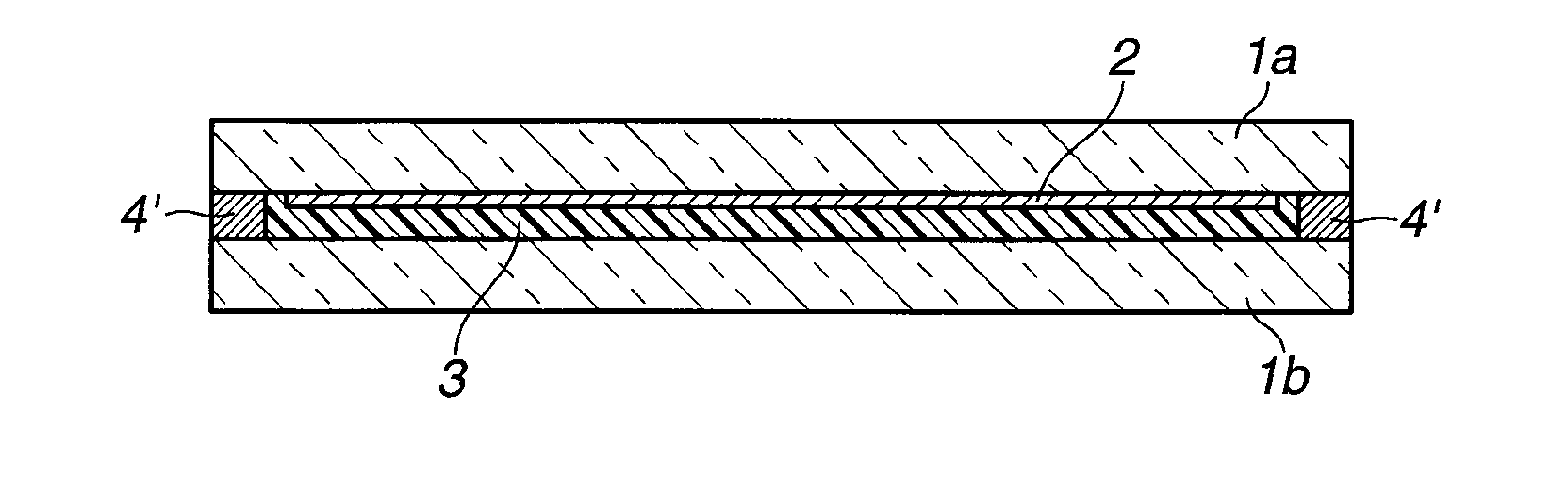
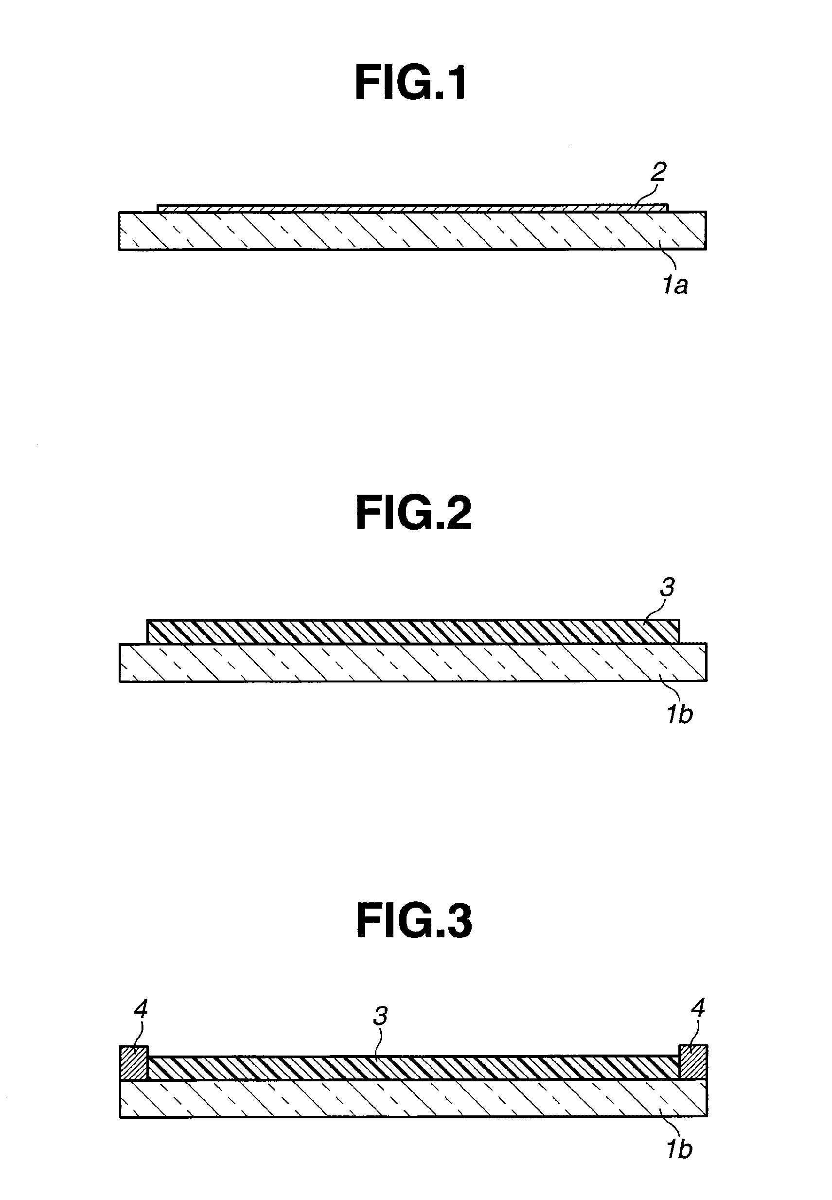
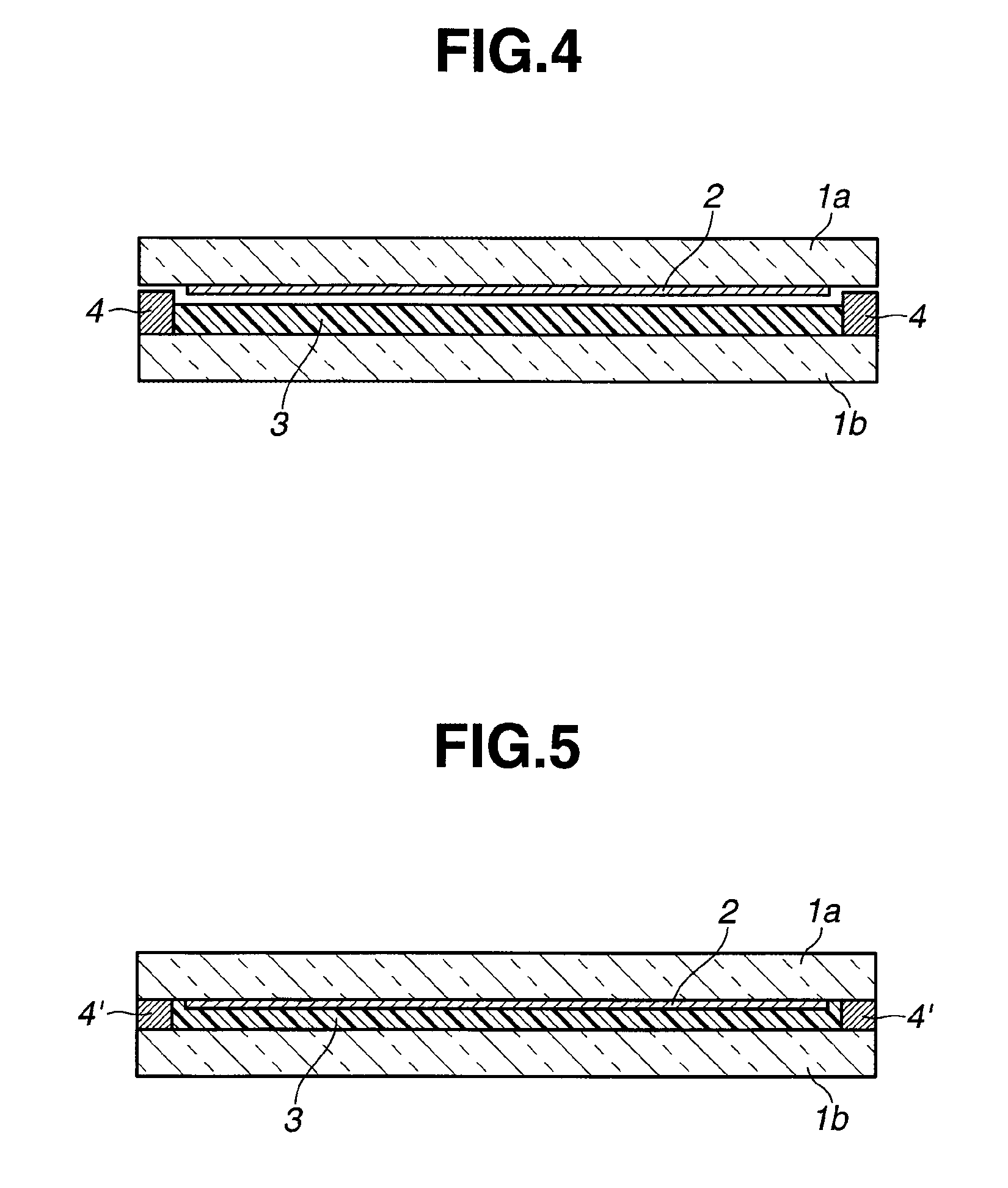
[0130]A second embodiment of the invention is a solar cell module comprising a transparent first substrate (panel 1a) having a surface, a thin-film solar cell (thin-film solar cell 2) comprising a light-transmissive electrode layer, a photoelectric conversion layer, and a metal electrode layer disposed on the surface of the first substrate in the described order, a second substrate (panel 1b) disposed above the surface of the first substrate, a silicone gel layer (silicone gel layer 3) interposed between the first and second substrates so as to overlap the thin-film solar cell, and a seal portion (seal portion 4′) comprising a water vapor non-permeable, rubber-based thermoplastic sealing material surrounding and sealing the outer periphery of the silicone gel layer.

[0131]The second embodiment differs from the first embodiment in that panel 1a is a transparent substrate (that is, identical with panel 1b in the first embodiment), that the layer structure of the thin-film solar cell 2 ...

example 1

[0144]There was furnished a first substrate or soda-lime glass plate of 1.8 mm thick and 22 cm squares. After a peripheral region of the first substrate was masked with a metal mask, constituent layers of a thin-film solar cell were deposited only on the inside region of 21 cm squares of the first substrate. Specifically, the first substrate was cleaned and the mask was laid on its surface. By the DC magnetron sputtering method, a Mo electrode film was deposited to a thickness of 0.8 μm. Then a CIGS layer of 2 μm thick was deposited by the three-stage evaporation method, a CdS buffer layer of 50 to 100 nm thick was deposited by the solution growth method, and a ZnO semi-insulating layer and an Al-doped ZnO transparent electrode layer were deposited by the sputtering method to a total thickness of 0.7 μm. Further, a MgF2 film of 120 nm thick was deposited by the vacuum evaporation method as antireflective film. An Al / Ni layer was formed by the vacuum evaporation method and processed ...


PUM


Abstract

A solar cell module is provided comprising a first substrate (1a), a thin-film solar cell (2) comprising a metal electrode layer, a photoelectric conversion layer, and a light-transmissive electrode layer disposed on the first substrate (1a), a transparent second substrate (1b) opposed to the solar cell on the first substrate, a light-transmissive silicone gel layer (3) interposed between the first and second substrates, and a seal (4′) of a water vapor non-permeable, rubber-based thermoplastic sealing material surrounding the outer periphery of the silicone gel layer. The module has long-term reliability and high efficiency.

Description

CROSS-REFERENCE TO RELATED APPLICATION[0001]This non-provisional application claims priority under 35 U.S.C. §119(a) on Patent Application No. 2013-135864 filed in Japan on Jun. 28, 2013, the entire contents of which are hereby incorporated by reference.TECHNICAL FIELD[0002]This invention relates to a solar cell module and a method for manufacturing the same. More particularly, it relates to a solar cell module having encapsulated therein a thin-film silicon solar cell or thin-film solar cell using a photoelectric conversion layer of compound semiconductors such as chalcopyrite and chalcogen compound semiconductors, e.g., copper-indium-gallium-selenide (CIGS) or copper-indium-selenide (CIS), and chalcogen semiconductor materials composed of Cd, Zn, Te, S and Se.BACKGROUND ART[0003]To provide solar cell modules with enhanced conversion efficiency and long-term reliability over 20 to 30 years or even longer, a number of reports and proposals relating to encapsulants were made in the a...

Claims


Application Information

Patent Timeline
IPC IPC(8): H01L31/18H01L31/048H01L31/20
CPCH01L31/0481H01L31/202H01L31/18H01L31/048Y02E10/541Y02P70/50Y02E10/50
Inventor ITO, ATSUOFURIHATA, TOMOYOSHIOHWADA, HIROTOKIM, HYUNG BAEYAGINUMA, ATSUSHIYAMAKAWA, NAOKIIGARASHI, MINORUHOTTA, MASAKATSUNAKAMURA, TSUTOMU
Owner SHIN ETSU CHEM CO LTD
Features
  • Generate Ideas
  • Intellectual Property
  • Life Sciences
  • Materials
  • Tech Scout
  • Unparalleled Data Quality
  • Higher Quality Content
  • 60% Fewer Hallucinations
Learn More