Photovoltaic device and method of manufacture

a photovoltaic device and manufacturing method technology, applied in the direction of electrolytic capacitor manufacturing, final product manufacturing, sustainable manufacturing/processing, etc., can solve the problems of long thermal process, unsatisfactory production, and long process time, so as to improve the throughput potential of the manufacturing process and contribute greatly to the scaling potential of the technology.

Inactive Publication Date: 2015-04-23
SWANSEA UNIV
View PDF4 Cites 2 Cited by
  • Summary
  • Abstract
  • Description
  • Claims
  • Application Information

AI Technical Summary

Benefits of technology

The present invention provides a method for manufacturing a counter electrode by depositing metal on a conductive substrate using near-infrared heating. The use of polyethylene glycol or ethyl cellulose as a binder makes the process easier to handle and screen print. The method is faster and more efficient compared to existing methods, improving throughput and scaling potential of the technology. The time required to deposit metal is significantly reduced, resulting in metal deposition over a much shorter time period.

Problems solved by technology

The heating is by way of a convection oven which is costly as the oven needs to be brought up to temperature and also it is also a lengthy process as typically the heat treatment is 30 minutes or more.
The printing of sensors and electrodes is becoming a more important way of manufacturing devices and because of the high throughput of these printing techniques, any lengthy thermal processes, especially those that slow down production is not desirable.

Method used


Image

  • Photovoltaic device and method of manufacture
  • Photovoltaic device and method of manufacture
  • Photovoltaic device and method of manufacture

Examples


Embodiment Construction

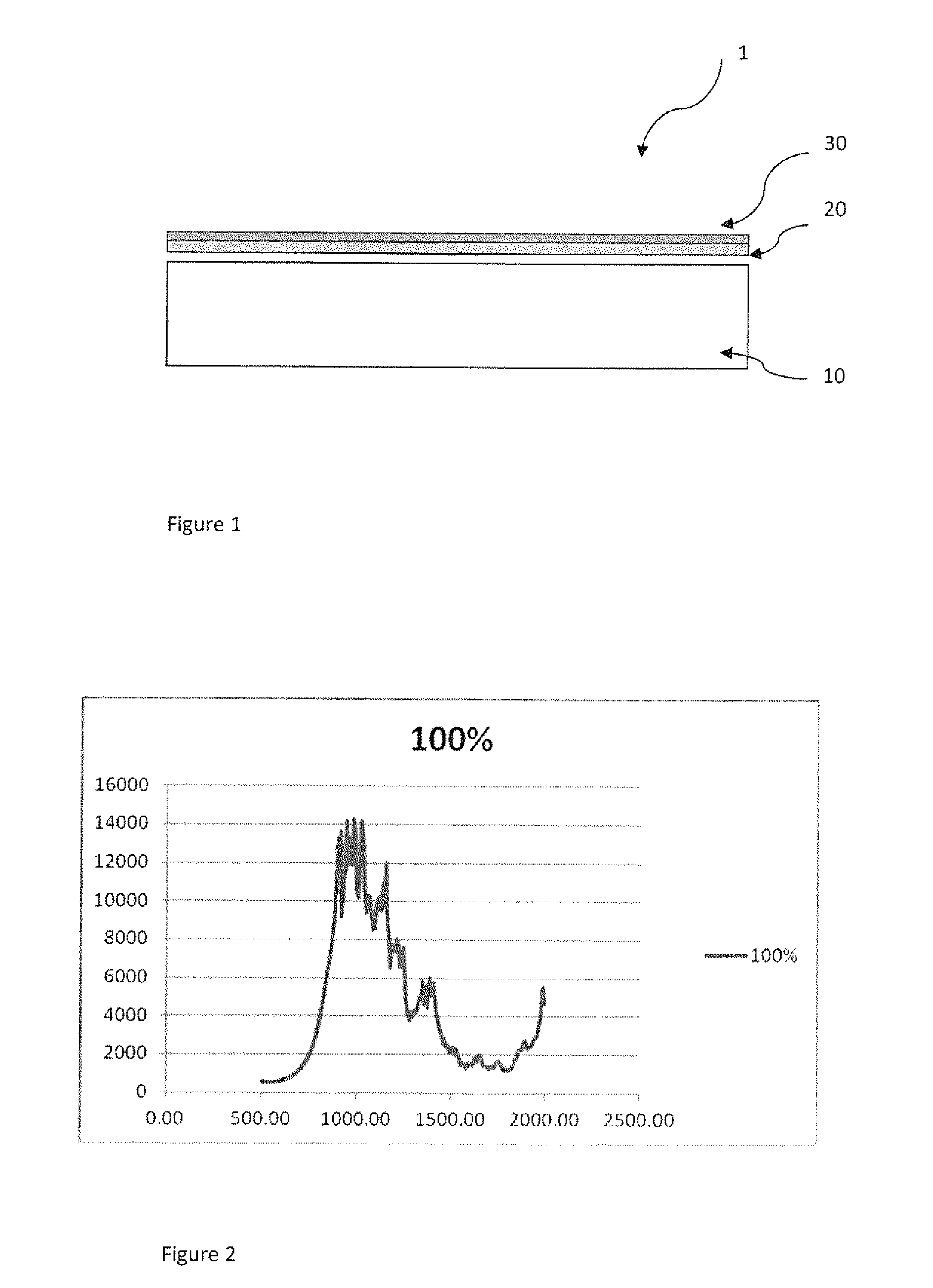
[0029]FIG. 1 shows an electrode 1 according to an embodiment of the invention. The electrode is formed of a glass substrate 10 on which is deposited a fluorine doped tin oxide 20. Overlaying the fluorine doped tin oxide layer is a layer of chloroplatinic acid 30 (5 Mm H2PtCl6(H2O)6)in iso proply alcohol which enables the layer to flow across the fluorine doped layer such as fluorine doped tin oxide. The flourine doped tin oxide layer, which renders the glass electrically conductive, absorbs significantly in the NIR and this allows for the subsequent heating of the Pt—Cl via a heat transfer process.

[0030]The platinum chloride layer was then treated with near infra-red radiation with a wavelength of 800 to 1500 nm and preferably 800 nm to 1000 nm. Although the layer includes platinum it is envisaged that other platinum group metals such as nickel or palladium may be used.

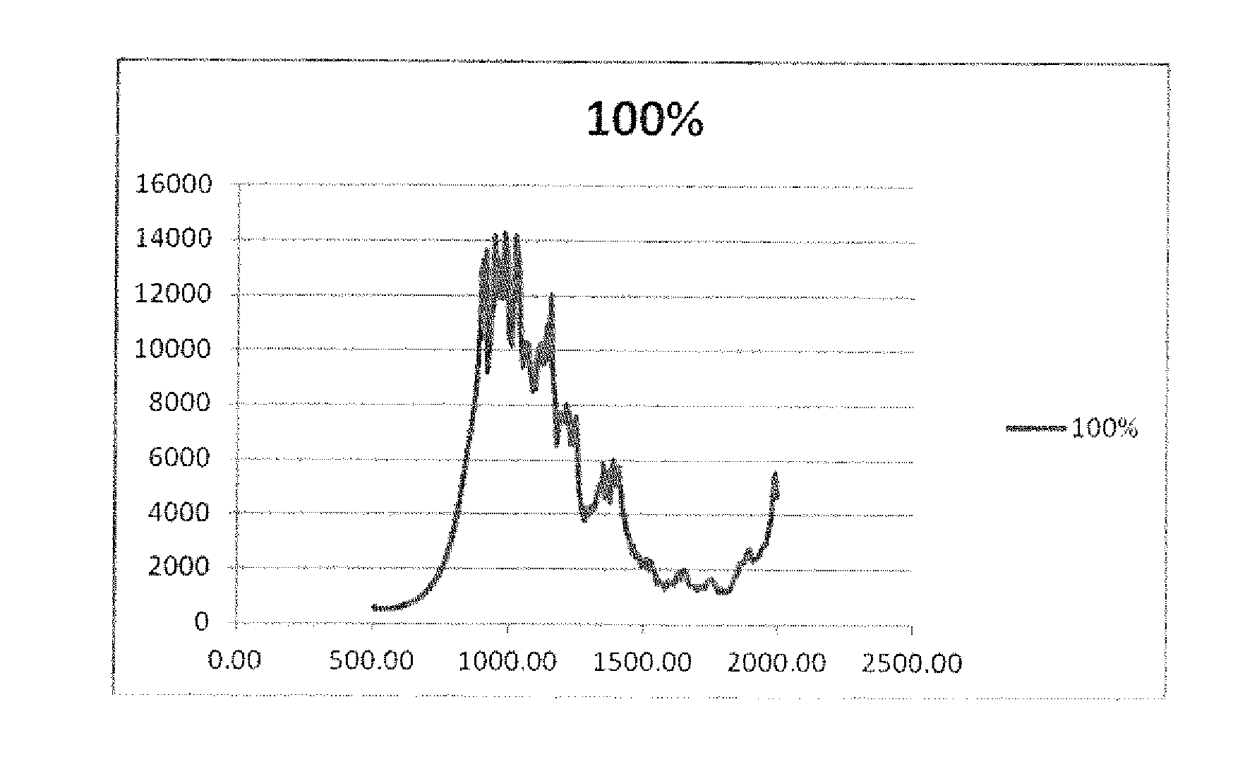
[0031]As shown in FIG. 2, the radiation is in the NIR spectrum and not the visible spectrum. The use of electromagn...


PUM

PropertyMeasurementUnit
Timeaaaaaaaaaa
Wavelengthaaaaaaaaaa

Abstract

A counter electrode generally shown as 1 is formed of a conductive substrate e.g. a glass substrate 10 on which is deposited doped oxide, e.g. a fluorine doped tin oxide 20. Overlaying the fluorine layer is a layer of a metal halide, e.g. platinum chloride 30 (5 Mm H2PtCl6(H2O6) in isoproply alcohol. Metal is deposited from the solution by treating with NIR. The tin oxide layer renders the glass electrically conductive, absorbs significantly in the NIR and allows for the subsequent heating of the Pt—Cl via a heat transfer process to make the counter electrode in a very efficient manner.

Description

FIELD OF THE INVENTION[0001]The invention relates to a photovoltaic device and a method of manufacture. In particular but not exclusively the device is a counter electrode for use in a dye sensitised solar cell (DSC)BACKGROUND OF THE INVENTION[0002]Dye sensitised solar cells (DSCs) typically consist of a working electrode and a counter electrode. The working electrode comprises a conductive substrate coated with a semi-conductive nanoparticulate metal oxide and a dye adsorbed onto the metal oxide to sensitize it to a larger portion of the solar spectrum. The counter electrode comprises a conductive layer and a catalytic material such as platinum deposited onto the conductive layer. The working electrode and the counter electrode may then be bonded together using sealants and spacers to form a well-defined space in which an electrolyte is housed.[0003]The electrolyte is usually an iodine / iodide redox couple in an organic solvent. A critical step in the manufacture of such DSCs is the...

Claims


Application Information

Patent Timeline
IPC IPC(8): H01G9/00H01G9/20
CPCH01G9/2022H01G9/0029H01G9/2031H01G9/2059Y02E10/542Y02P70/50C23C18/08C23C18/14
Inventor WATSON, TRYSTANWORSLEY, DAVIDCHARBONNEAU, CECILE
Owner SWANSEA UNIV
Why Eureka
Try Eureka