The grain boundaries and dislocations that are created during growth or that arise later due to stresses in the material typically lead to a reduced performance.
The
anisotropic etching process described above does not provide such benefits in the context of a multi-crystalline
wafer, which displays no consistency in the orientation of the crystalline structure.
These tend to create an irregular surface texture, which is less efficient in terms of light absorption than the regular pyramidal structure available with
anisotropic etching applied to a {100} crystallographic plane.
However, the production of large volumes of wafers for use in photovoltaic cells by this process is found to be relatively expensive as the volume of crystalline silicon that can be produced in a single run of the process is relatively small in practice.
Oxygen impurities are known be detrimental to the performance of silicon solar cells.
Although the use of a seed material in directional solidification processes has been found to offer some success in the growth of mono-crystalline material, it is not completely effective or attractive.
This multi-crystalline part of the ingot is inherently less electrically efficient when used for its purpose in photovoltaic cells than the mono-crystalline part of the ingot, and in face has been found to offer worse performance than standard multi-crystalline material.
Moreover, the multicrystalline part is inappropriate for the
anisotropic etching process described above.
As well as limiting the light absorbing efficiency of the wafers and offering a reduced
electrical performance, this latter point also leads to a major undesirable visual difference between etched regions in the
wafer that are formed of mono-crystalline material and those that are formed of multi-crystalline material.
This very visible inhomogeneity means that it is difficult for manufacturers of solar modules to use such wafers in a module, since customers prefer modules which appear homogenous.
Another
disadvantage of the incursion of multi-crystalline regions into the ingot comes in the formation of the silicon wafers from the ingot.
However, the grain boundaries, defects and dislocations of the multi-crystalline silicon frequently allow impurities such as
silicon carbide to become embedded in the ingot.
Such impurities not only decrease the efficiency of the material further, but are also relatively hard, and can break the
diamond wire during
cutting.
As a result, the multi-crystalline regions can cause less optimal
cutting processes to be required.
This problem is particularly acute when forming ingots using a mono-crystalline seed.
This is because the increased time necessary in the process to carefully control the melting of the silicon feedstock without fully melting the seed material offers an
increased risk of
contamination of the
molten material by carbon.
However, it is extremely difficult to control a process of this kind.
For example, given that, prior to solidification,
molten silicon is provided in the crucible all the way down the seed material placed on the crucible floor, it is 1-5 difficult to ensure that the seed material on the side walls does not melt.
Melting of the seed material renders it ineffective since its crystalline structure is lost.
However, in practice such processes suffer from numerous disadvantages, such as
increased stress in the ingot which will make it more likely to crack and increased frequency of defects such as twin grain boundaries and dislocations.
Moreover, the heat added to the side walls of the crucible represents a cost in terms of energy use and is difficult to implement without melting the seed material.
Furthermore, implementation of these processes will slow down
crystal growth and productivity.


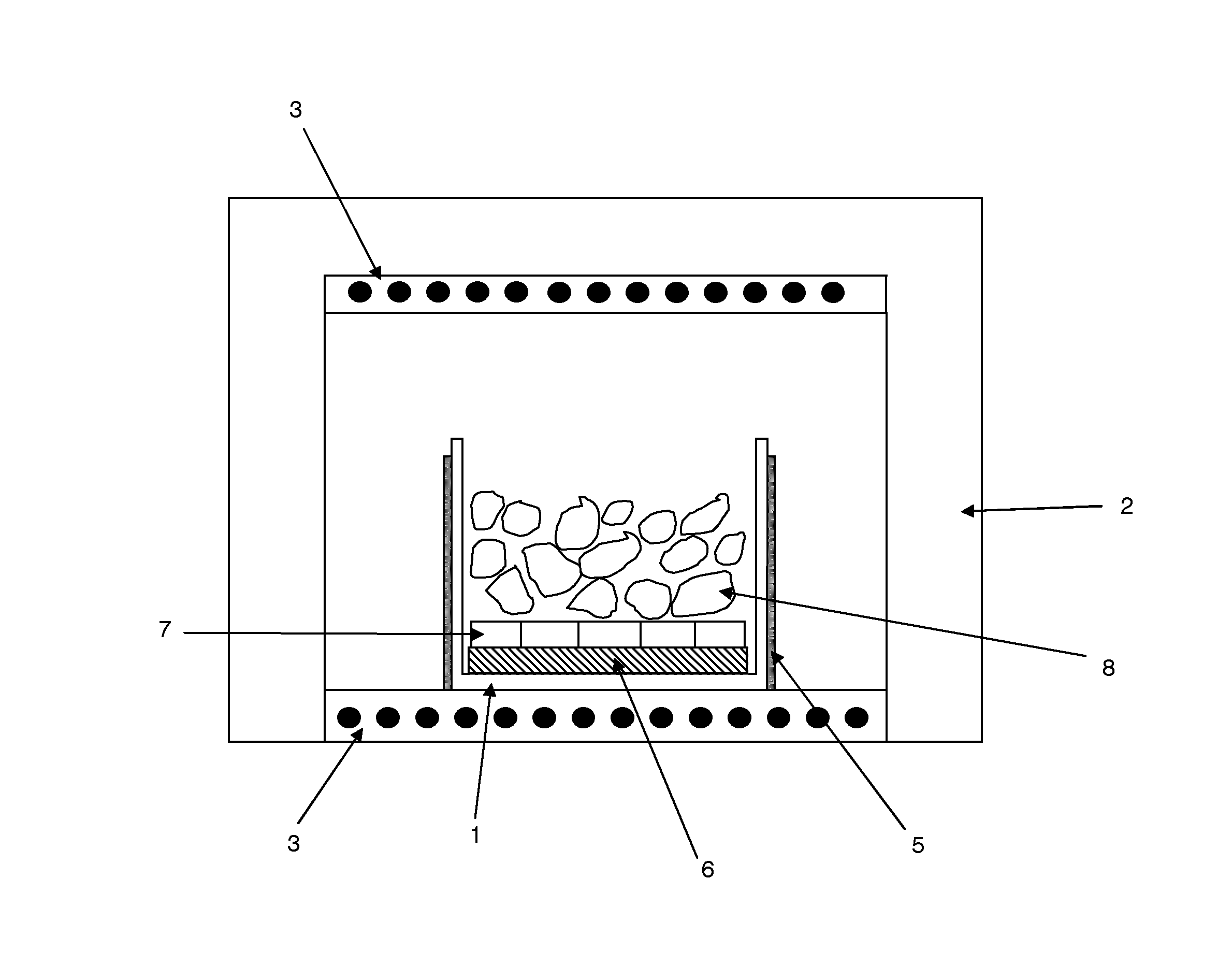
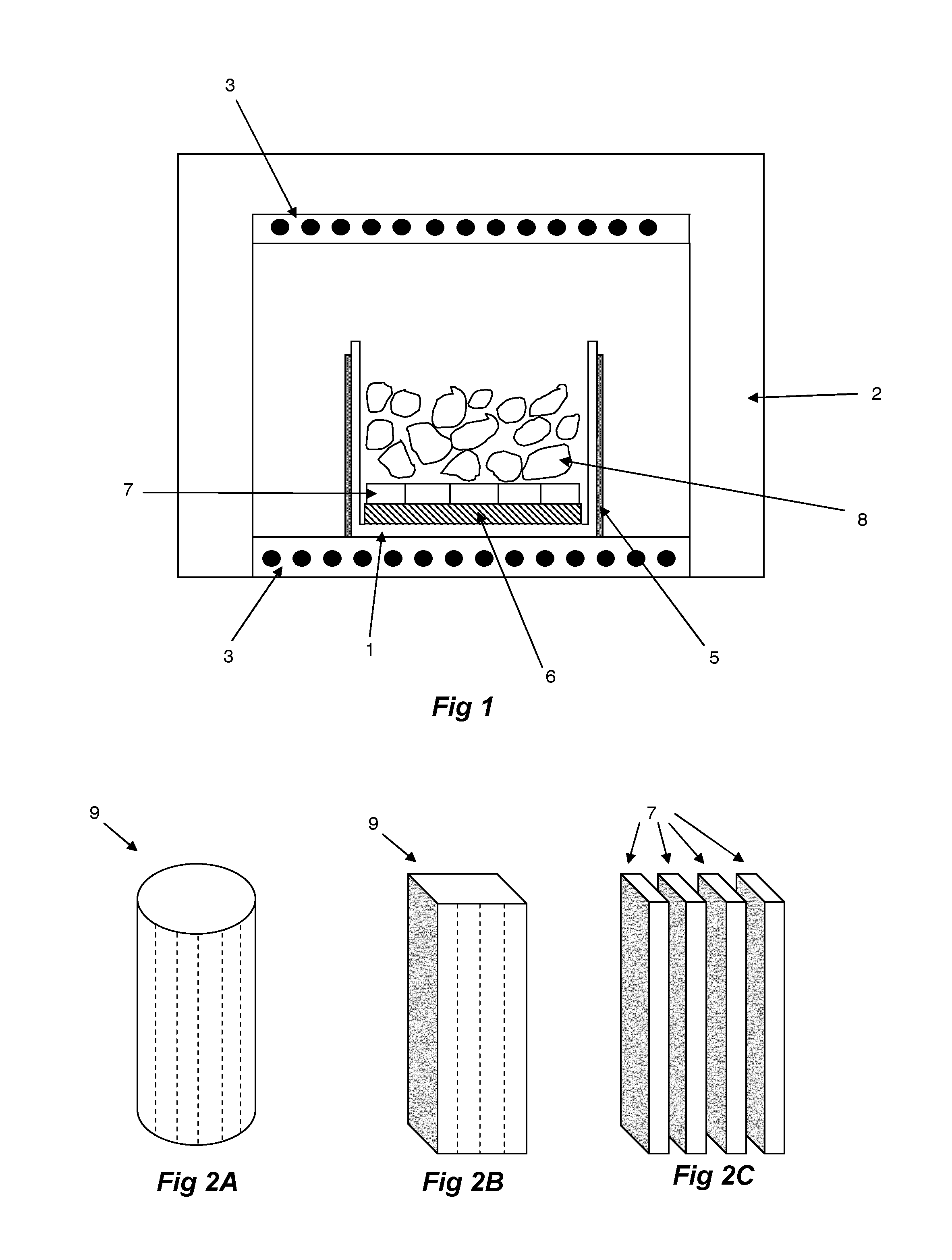
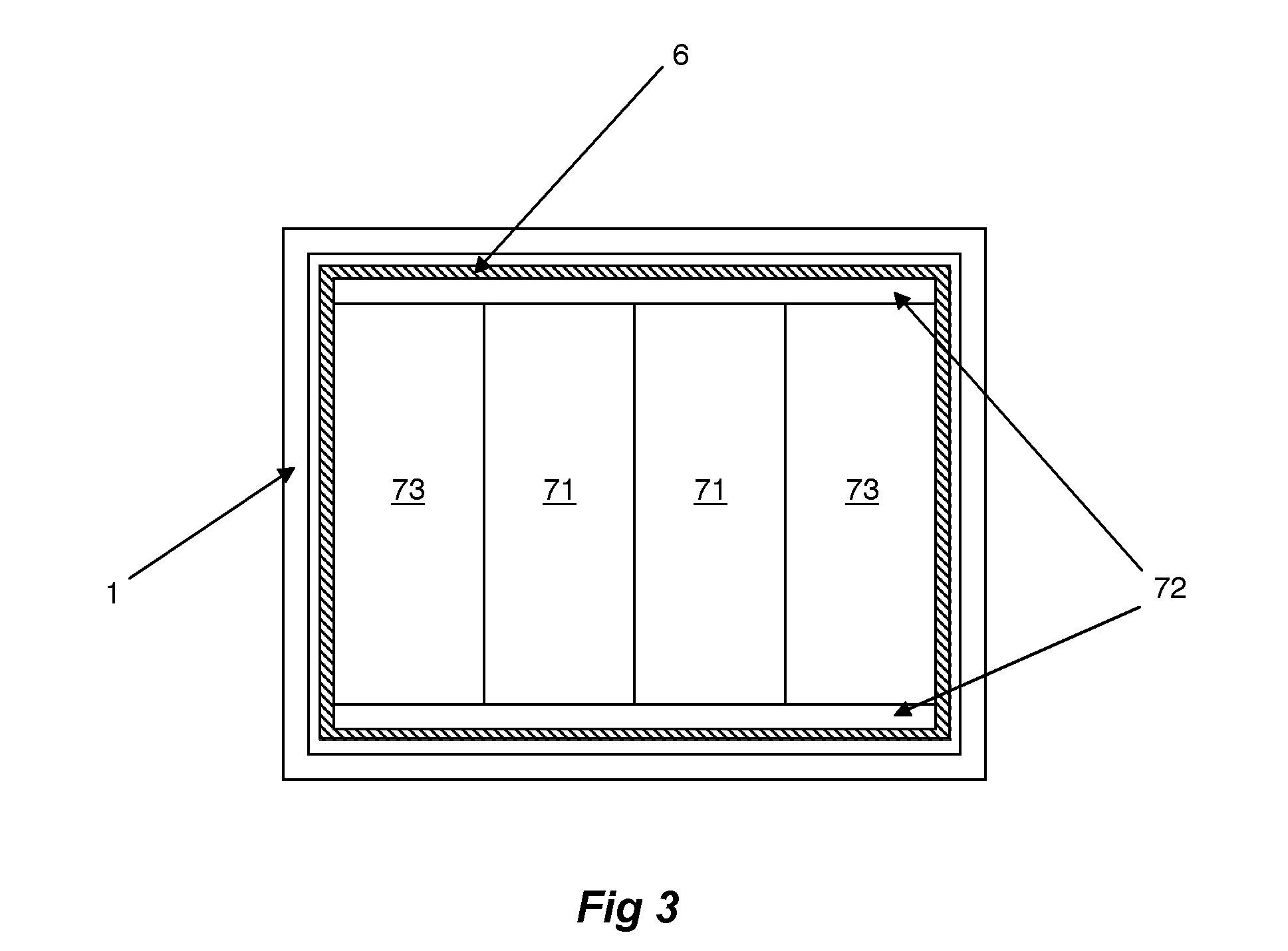