Thin film transistor and display device

Active Publication Date: 2015-06-18
KOBE STEEL LTD
View PDF4 Cites 6 Cited by
  • Summary
  • Abstract
  • Description
  • Claims
  • Application Information

AI Technical Summary

Benefits of technology

[0021]The present invention can provide a thin film transistor having excellent switching characteristics and stress stability shown by a small variation of threshold voltage before and after applying the light irradiation and the electrically negative biasing as well as a small variation of threshold voltage before and after

Problems solved by technology

When a thin film transistor is used, such variation of the switching characteristics due to the stress by the voltage application and the light irradiation causes deterioration of reliability in a display devices itself.
Similarly in an organic EL display panel, the semiconductor layer is irradiated by light leaked out from a light emission layer, causing problems as a variation and a deviation of the threshold voltage in the TFT.
Such a shift of threshold voltage of the TFT particularly deteriorates the reliability o

Method used


Image

  • Thin film transistor and display device
  • Thin film transistor and display device

Examples


example 1

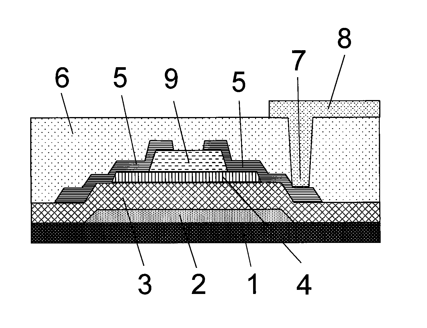
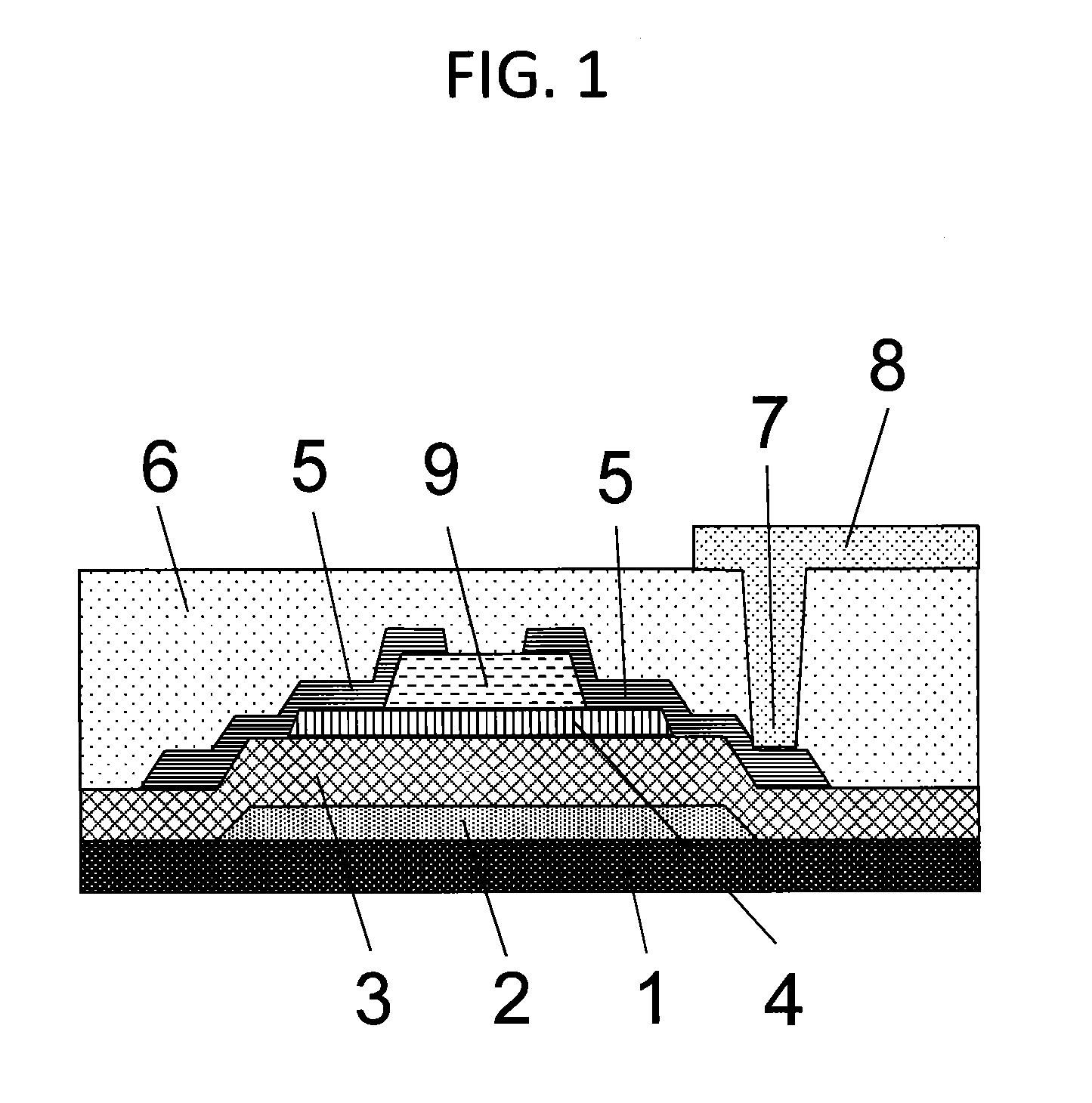
[0075]Thin film transistors shown in FIG. 1 were fabricated as described below, and their stress stability and other characteristics were evaluated. It is noted here that a transparent conductive film 8 was not deposited in the present Example. First, a Mo thin film of 100 nm in thickness as a gate electrode 2 and SiO2 film of 250 nm in thickness as a gate insulator film 3 were successively deposited on a glass substrate 1 (“EAGLE 2000” available from Corning Inc, having a diameter of 100 mm and a thickness of 0.7 mm). The gate electrode 2 was deposited using a pure Mo sputtering target by a DC sputtering method under the conditions: deposition temperature, room temperature; sputtering power density, 3.8 W / cm2; carrier gas, Ar; gas pressure, 2 mTorr; Ar gas flow rate, 20 sccm.

[0076]Further, the gate insulator film 3 was formed by a plasma CVD method using a mixed gas of SiH4 and N2O with a carrier gas. Specifically, single layers of the gate insulator film 3 were deposited on a roun...

example 2

[0135]Thin film transistors shown in FIG. 1 with a two-layered gate insulator film 3 were fabricated as described below, and their stress stability and other characteristics were evaluated. It is noted here that a transparent conductive film 8 shown in FIG. 1 was not deposited in the present Example.

[0136]Firstly, a Mo thin film of 100 nm in thickness was deposited as a gate electrode 2 on a glass substrate 1. On the gate electrode 2, a lower layer of the gate insulator film 3 of SiOx (SiO2) or SiNx (SiN) on the side of the gate electrode was formed, followed by a deposition of an upper layer of the gate insulator film 3 of SiOx (SiO2) which comes to the side of the oxide semiconductor layer. Each of the layers of the gate insulator film 3 was deposited by a plasma CVD method on a round shape electrode of 8 inches in diameter (total area of 314 cm2) as an electrode of an CVD apparatus. Specifically, when a SiO2 film was formed as the layer on the side of the gate electrode in the ga...


PUM


Abstract

Provided is a thin film transistor comprising an oxide semiconductor thin film layer and has a threshold voltage that does not change much due to light, a bias stress or the like, thereby exhibiting excellent stress stability. A thin film transistor of the present invention is provided with: a gate electrode; an oxide semiconductor layer that is used as a channel layer; and a gate insulator film that is arranged between the gate electrode and the channel layer. The oxide semiconductor layer is configured of at least one metal element that is selected from the group consisting of In, Ga, Zn and Sn (excluding the cases where the oxide semiconductor layer is constituted of metal elements Sn, and at least one of In and Zn). The hydrogen concentration in the gate insulator film, which is in direct contact with the oxide semiconductor layer, is controlled to 4 atomic % or less.

Description

TECHNICAL FIELD[0001]The present invention relates to a thin-film transistor (TFT) to be used in display devices such as liquid crystal displays and organic EL displays; and a display device having the thin-film transistor.BACKGROUND ART[0002]As compared with widely used amorphous silicon (a-Si), amorphous (non-crystalline), oxide semiconductors have high carrier mobility (also called as field-effect mobility, which may hereinafter be referred to simply as “mobility”), a wide optical band gap, and film formability at low temperatures, and therefore, have highly been expected to be applied for next generation displays, which are required to have large sizes, high resolution, and high-speed drives; resin substrates having low heat resistance; and others (see Patent Document 1).[0003]Among the oxide semiconductors, amorphous oxide semiconductors consisting of indium, gallium, zinc and oxygen (In-Ga-Zn-O, which may hereinafter be referred to as “IGZO”) have preferably been used in parti...

Claims


Application Information

Patent Timeline
IPC IPC(8): H01L29/786
CPCH01L29/7869G02F1/1362H01L29/66742H01L29/786H10K59/00H01L21/02126H01L21/02164H01L21/0217H01L29/78606H01L2924/13069H10K59/1213H01L21/823462
Inventor MIKI, AYAMORITA, SHINYAGOTO, HIROSHIKUGIMIYA, TOSHIHIROTAO, HIROAKIHIROSE, KENTA
Owner KOBE STEEL LTD
Why Eureka
Try Eureka