Methods, Apparatuses, Systems and Software for Treatment of a Specimen by Ion-Milling

a technology of ion milling and specimens, applied in the field of ion milling, can solve the problems of insufficient bib and pfib techniques for planar delayering for micromachining purposes, lack of real-time control and site-specific capabilities, etc., and achieve excellent process accuracy, high quality processing and results, and increased speed

Active Publication Date: 2015-09-10
IB LABS
View PDF8 Cites 20 Cited by
  • Summary
  • Abstract
  • Description
  • Claims
  • Application Information

AI Technical Summary

Benefits of technology

[0017]The present invention enables planar site-specific delayering at both chip and wafer levels, nanometer-level depth resolution, increased speeds (e.g., order-of-magnitude) relative to existing methods, real-time process control, end-point detection and automation, and ability to integrate with existing analytical techniques. The present apparatus and / or system spans applications ranging from focused ion beam (FIB) to broad ion beam (BIB), and enables in situ ion beam milling and imaging. The present micro-machining apparatus, system and method provide a convenient platform for failure analysis and 3D metrology in fields from microelectronics to materials science (e.g., for layer-by-layer materials analysis, or chemical composition and contamination analysis when combined with analytical tools) to life sciences. The present apparatus and system are amenable to an open-concept modular design, and are configurable as a stand-alone instrument or integratable into existing scanning electron microscopes, FIBs, mass spectrometers, Raman spectrometers, and other analytical tools.
[0018]The present system and / or apparatus, which may be referred to herein as a “Universal Ion Beam (UIB)” machining system, is designed for site-specific planar polishing and micromachining, among other functions and applications. The inventive process is optimized for in situ delayering, sample preparation for scanning election microscopy (SEM) and tunneling election microscopy (TEM), and / or post-FIB final cleaning. The present system, apparatus, and method provide high quality processing and results. For example, curtaining, amorphization and other ion-induced artifacts (e.g., by gallium or other relatively heavy ions) can be minimized or eliminated. The present system, apparatus, and method can also provide excellent process accuracy. For example, the process, including endpoint monitoring, can be provided by high-resolution / high-sensitivity imaging and / or analytical optical or electronic signal control (e.g., for surface analysis). Examples of such imaging and / or analytical optical / electronic signal control techniques include interferometry, spectroscopic reflectometry, electron back-scattering, mass spectrometry, XPS, Auger spectroscopy, etc. The present system, apparatus, and method provide relatively high throughput. For example, 4-10 TEM / STEM samples per 8-12 hour period (e.g., a typical work shift in a failure analysis lab) can be processed using the present invention. The present system, apparatus, and method are applicable to a variety of applications and sample preparation modes. Automated control of process accuracy, quality and termination can also be achieved by the present system, apparatus, and method.
[0019]Major features of the present ion milling apparatus include substantially unlimited beam positioning and maneuvering over a stationary sample, which enables true real time process control during substantially the entire course of ion milling (enabled by the stationary sample), high quality planar milling (enabled by the azimuthal beam and maneuverability thereof), sputtering rate control (enabled by the variable incidence angle of the ion beams), and a wide range of beam sizes from focused (tens of nm) to broad (mm range) enabled by the beam optics. The design and / or architecture of the present apparatus enables use of a combination of swappable ion sources in a single machine for best choice of the ion for a particular milling application (e.g., a liquid metal ion beam can be used for high precision FIB, a xenon or argon ion beam can be used for a high current beam, or one or more cluster gas ion beams can be used to provide atomic level surface smoothness of the sample).

Problems solved by technology

Conventionally, delayering methods in semiconductor and integrated circuit metrology and failure analysis include laborious, repetitive, and arguably blind polishing steps by general mechanical or RIE-polishing, followed by meticulous SEM inspection in between such steps.
However, FIB and PFIB techniques are generally insufficient for planar delayering for micromachining purposes, because of limitations in achieving nanometer scale roughness and planarity when treating different materials in the same sample.
However, BIB generally lacks real-time control and site-specific (e.g., target alignment and beam precision) capabilities.
Even more broadly, general polishing and RIE are inefficient, not site-specific, and generally require intermittent external microscope observations to determine progress.
No techniques are known to the inventors that provide site-specific planar delayering solutions at the wafer level.
Thus, there is generally a lack of efficient, controlled and reliable site-specific delayering techniques and tools for advanced 45-10 nm nodes in semiconductor and / or integrated circuit metrology and / or failure analysis.

Method used


Image

  • Methods, Apparatuses, Systems and Software for Treatment of a Specimen by Ion-Milling
  • Methods, Apparatuses, Systems and Software for Treatment of a Specimen by Ion-Milling
  • Methods, Apparatuses, Systems and Software for Treatment of a Specimen by Ion-Milling

Examples


Embodiment Construction

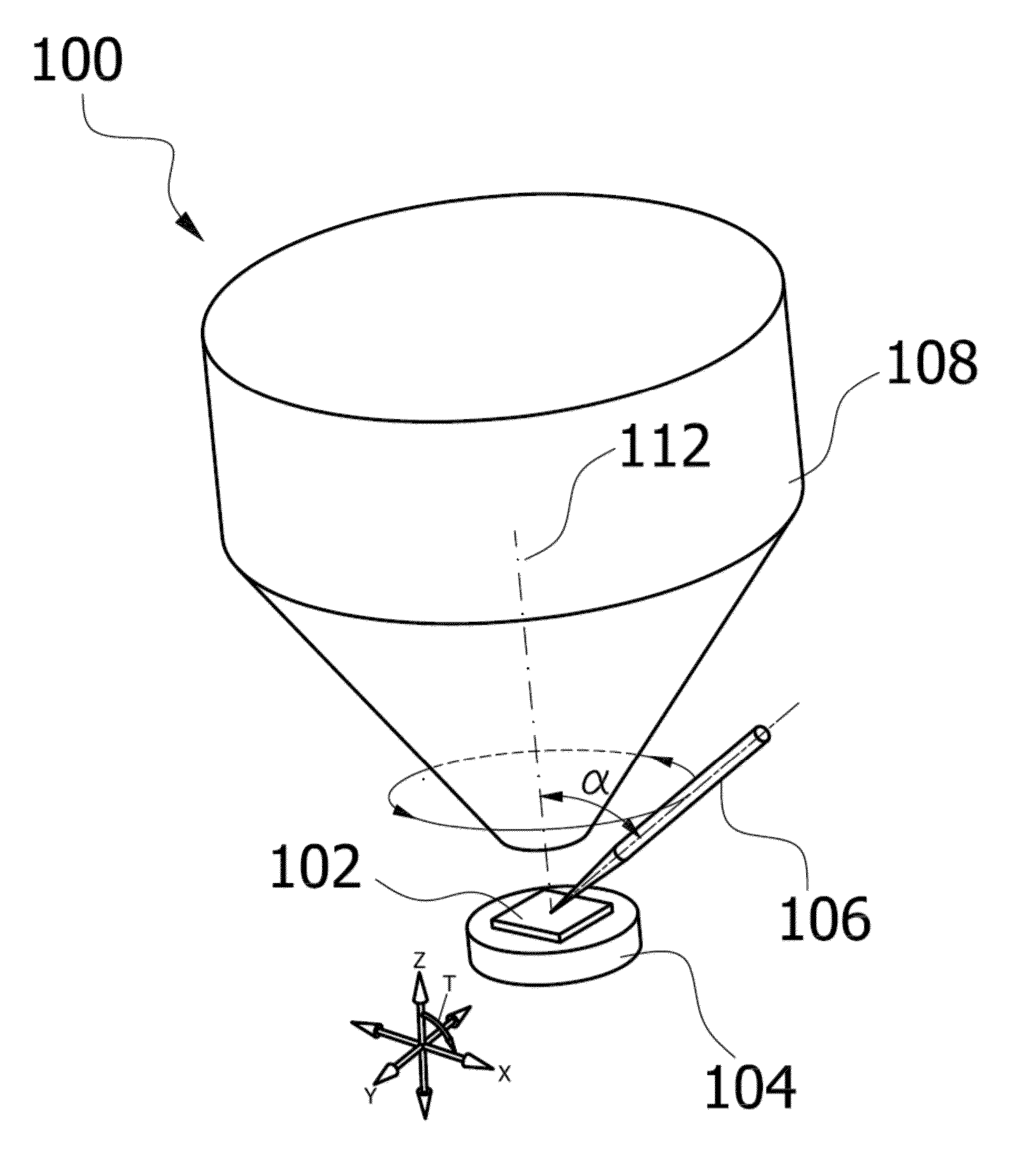
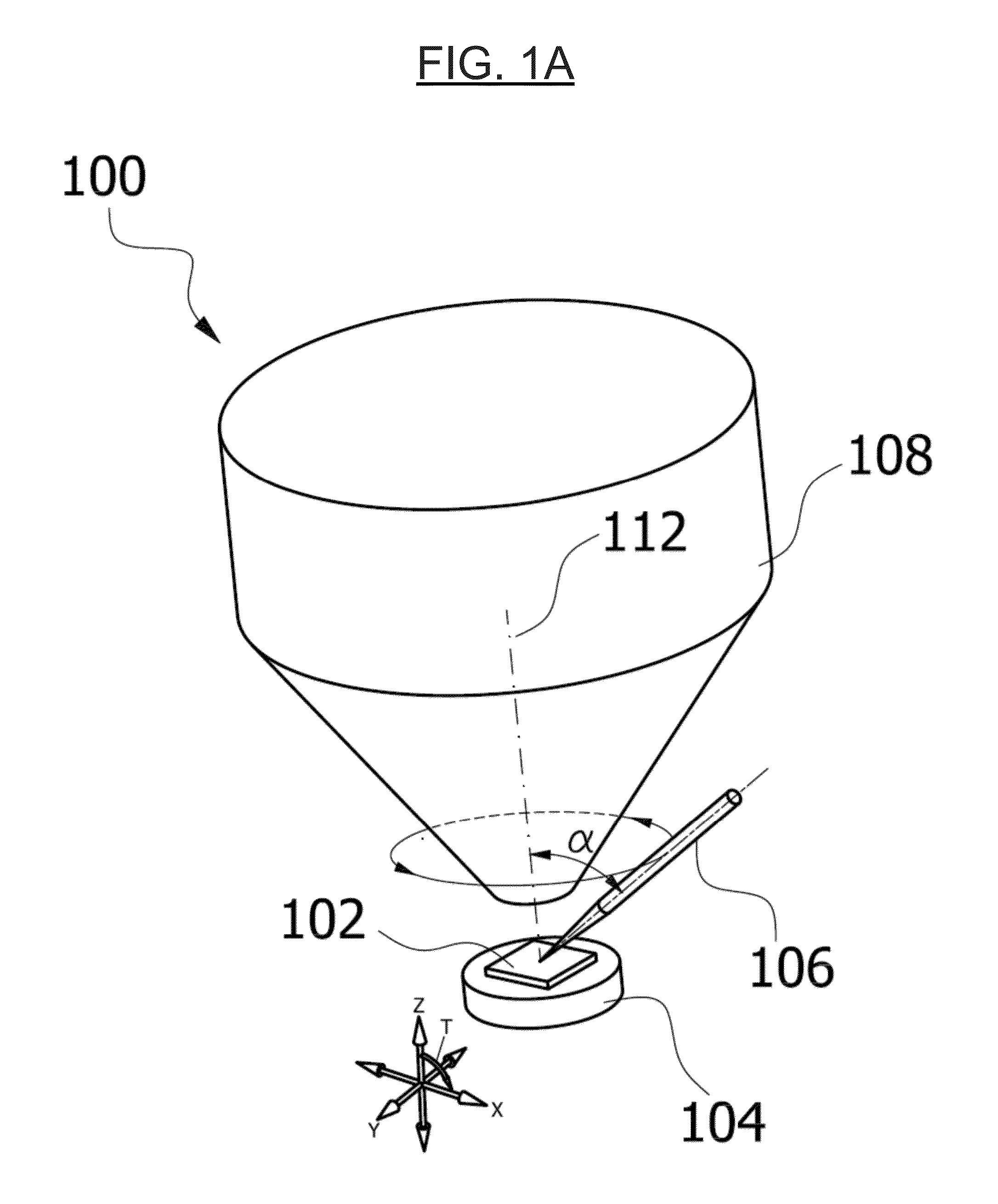
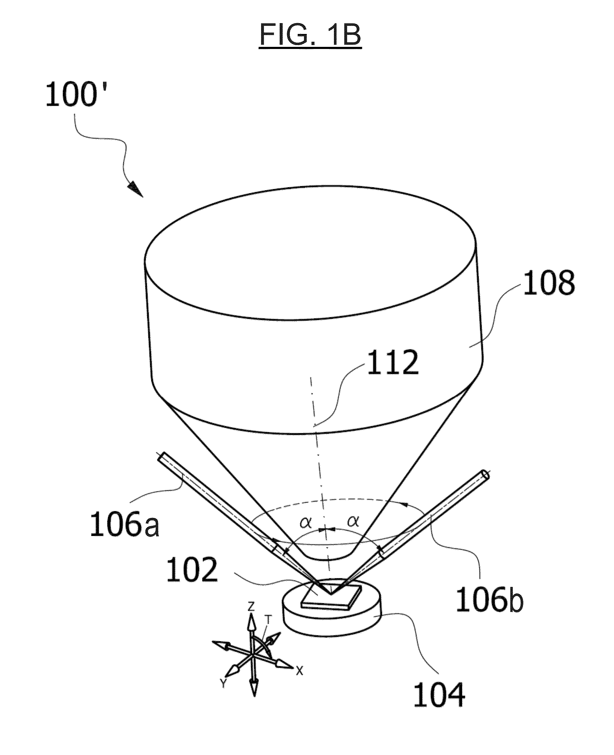
[0046]Reference will now be made in detail to various embodiments of the invention, examples of which are illustrated in the accompanying drawings. While the invention will be described in conjunction with the following embodiments, it will be understood that the descriptions are not intended to limit the invention to these embodiments. On the contrary, the invention is intended to cover alternatives, modifications and equivalents that may be included within the spirit and scope of the invention as defined by the appended claims. Furthermore, in the following detailed description, numerous specific details are set forth in order to provide a thorough understanding of the present invention. However, it will be readily apparent to one skilled in the art that the present invention may be practiced without these specific details. In other instances, well-known methods, procedures, components, and circuits have not been described in detail so as not to unnecessarily obscure aspects of th...


PUM

PropertyMeasurementUnit
angleaaaaaaaaaa
anglesaaaaaaaaaa
timeaaaaaaaaaa

Abstract

Methods, apparatuses, systems and software for ion beam milling or machining are disclosed. The apparatus includes a specimen holder, a table, one or more ion sources, rotatable ion optics, and an imaging device. The specimen holder is configured to hold a specimen in a stationary position during milling or machining. The table is configured to change the stationary position of the specimen holder in any of three orthogonal linear directions and an angular direction. The rotatable ion optics are configured to emit an ion beam towards a predetermined location on the specimen from any of the one or more ion sources at any angle around an axis that is orthogonal to a horizontal surface of the table when the angular direction of the table is 0°. The imaging device is configured to generate an image of the specimen including the predetermined location, thereby enabling real-time monitoring of the milling or machining process.

Description

RELATED APPLICATIONS[0001]This application claims the benefit of U.S. Provisional Pat. Appl. No. 61 / 950,109, filed Mar. 9, 2014, pending, which is incorporated herein by reference in its entirety.FIELD OF THE INVENTION[0002]The present invention generally relates to the field of ion milling (e.g., surface and 3D treatment of specimen at atomic depth resolution by ion-milling), with and without laser beam assistance. More specifically, embodiments of the present invention pertain to methods, apparatuses, systems and software for ion milling a specimen that can be used in the fields of semiconductors, materials science, nanotechnology, and life science, among other fields.DISCUSSION OF THE BACKGROUND[0003]Conventionally, delayering methods in semiconductor and integrated circuit metrology and failure analysis include laborious, repetitive, and arguably blind polishing steps by general mechanical or RIE-polishing, followed by meticulous SEM inspection in between such steps. The average...

Claims


Application Information

Patent Timeline
Patent Type & Authority Applications(United States)
IPC IPC(8): H01J37/305G01N1/32
CPCH01J37/3056H01J2237/31745G01N1/32H01J37/147H01J37/20H01J2237/0245H01J2237/0827H01J2237/1505H01J2237/31749
Inventor BOGUSLAVSKY, DIMITRYKOVLER, MARK
Owner IB LABS
Why Eureka
Try Eureka