Vertical cavity surface emitting lasers with silicon-on-insulator high contrast grating

a laser and silicon-on-insulator technology, applied in the direction of semiconductor laser structure details, semiconductor lasers, semiconductor laser arrangements, etc., can solve the problems of many problems, and achieve the effect of low cost manufacturing

Inactive Publication Date: 2015-10-08
RGT UNIV OF CALIFORNIA
View PDF5 Cites 27 Cited by
  • Summary
  • Abstract
  • Description
  • Claims
  • Application Information

AI Technical Summary

Benefits of technology

[0013]The present invention provides apparatus and methods for fabricating surface-emitting laser devices, and more particularly surface-emitting laser devices within an array of surface-emitting laser devices in an integrated circuit, in which the wavelengths of the individual surface-emitting laser devices can be individually selected. There are a number of benefits to providing arrays of devices operating at multiple wa

Problems solved by technology

However, many problems arise when trying to fabricate VCSELs having a span of wavelengths on a single chip.
In particular, many problems arise i

Method used


Image

  • Vertical cavity surface emitting lasers with silicon-on-insulator high contrast grating
  • Vertical cavity surface emitting lasers with silicon-on-insulator high contrast grating
  • Vertical cavity surface emitting lasers with silicon-on-insulator high contrast grating

Examples


embodiment 10

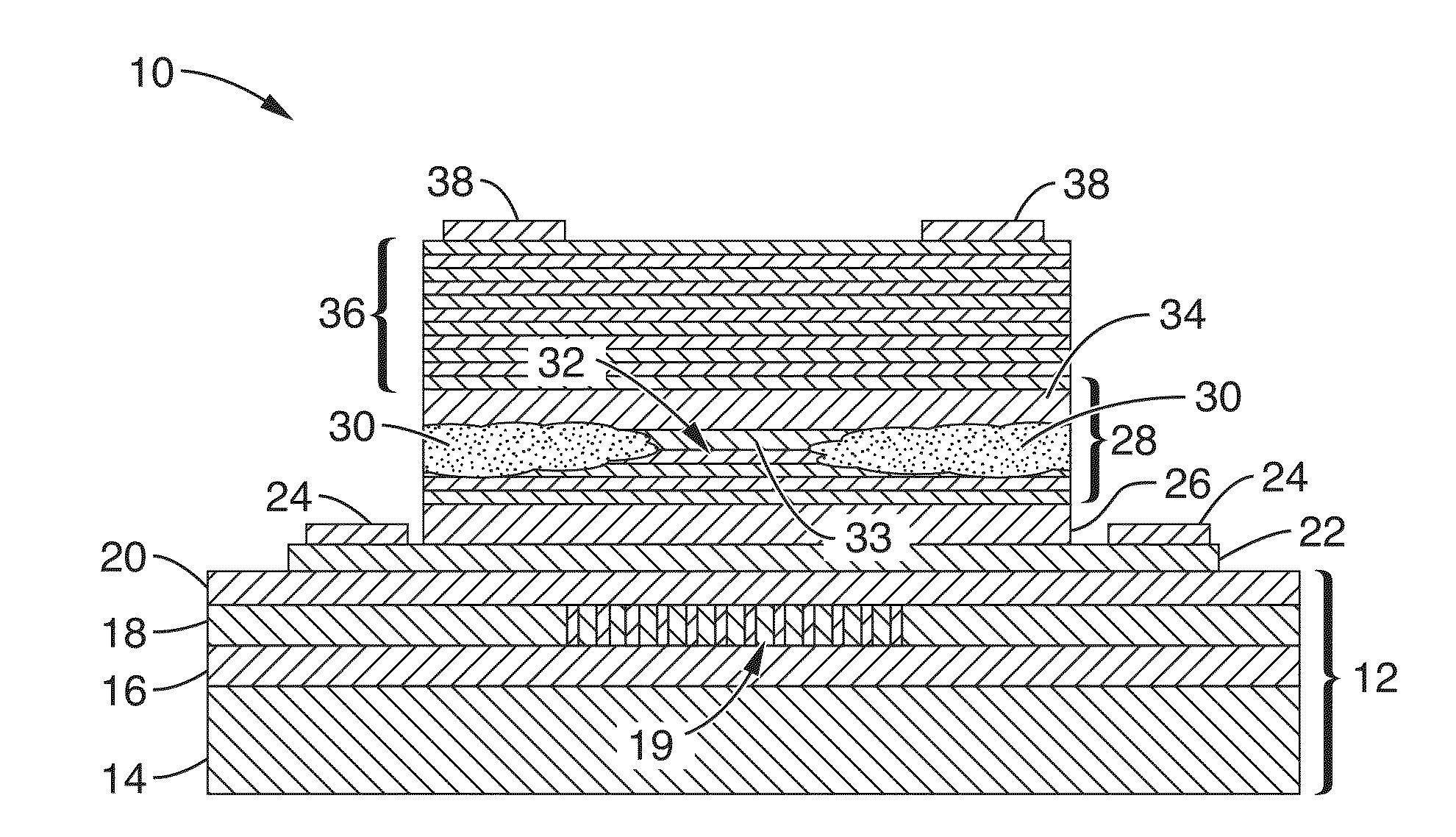
[0036]FIG. 1 illustrates an embodiment 10 of a silicon on insulator (SOI) form of high contrast grating (HCG) VCSEL, showing a specially adapted SOI substrate 12 upon which the remainder of the VCSEL is fabricated. It should be appreciated that silicon on insulator (SOI) technology is known to refer to the use of a layered silicon-insulator-silicon substrate in place of conventional silicon substrates in semiconductor manufacturing. A typical SOI substrate contains a layer of silicon dioxide at a predetermined depth within a silicon wafer. An SOI-based device differs from conventional silicon-based devices in that the silicon layer is above an electrical insulator, typically silicon dioxide, or sapphire in the case of the similar silicon on sapphire (SOS) substrates. The inclusion of the buried insulator layer provides a necessary cladding, so as to prevent light leakage to the silicon layer. Selection of insulator type depends largely on intended application and cost factors, with ...

embodiment 50

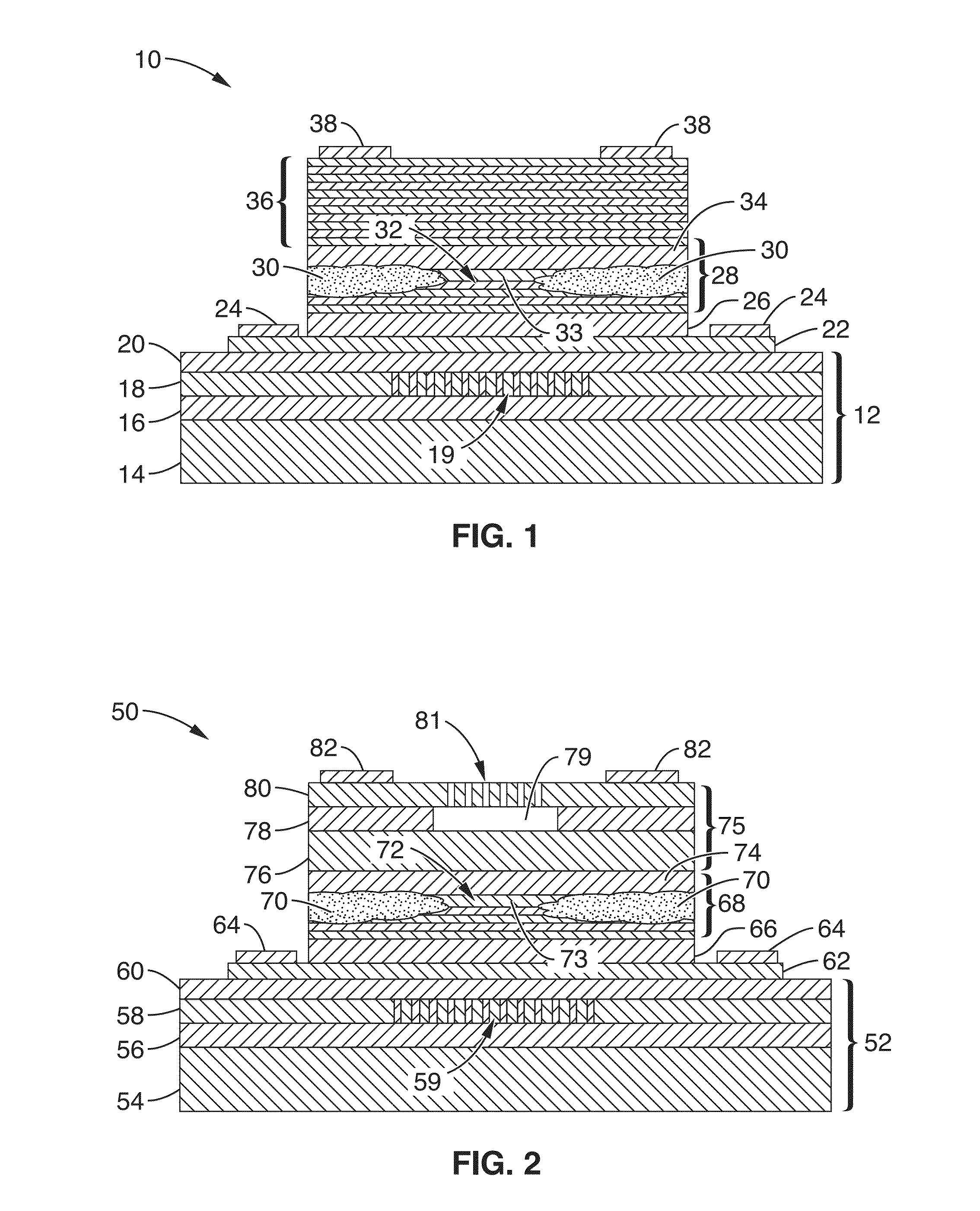
[0041]FIG. 2 illustrates a similar SOI HCG VCSEL embodiment 50, which utilizes an HCG for a top mirror instead of the DBR layers. A specially adapted SOI substrate 52 is shown as comprising a base layer 54 (e.g., Si), a lower spacer layer 56 (e.g., SiO2), a grating layer 58 (e.g., grating patterned Si) with periodic spaced apart segments 59 of Si, and an upper spacer layer 60. The top half of the VCSEL (above the SOI-like HCG patterned substrate) contains the contact and current spreading layers, the active region, and the top mirror. A contact layer 62 is provided upon which a contact 64 is formed. A current spreading layer 66 is provided for creating a current spreading path above contact layer 62. An active portion 68 contains the active region 74 and is also preferably configured for current confinement. The active portion 68 can incorporate optional DBR layers to extend the current spreading path. An optional tunnel junction (not shown) can be formed within active portion 68. O...

embodiment 1

[0074]2. The apparatus of embodiment 1, wherein said upper mirror reflector comprises a high contrast grating (HCG).

[0075]3. The apparatus of embodiment 1, wherein said upper mirror reflector comprises a distributed Bragg reflector (DBR).

[0076]4. The apparatus of embodiment 1, wherein said lower mirror reflector comprises Si segments forming a sub-wavelength high contrast grating (HCG).

[0077]5. The apparatus of embodiment 1, wherein said half-VCSEL structure comprises compounds selected from group III-V or II-VI compounds


PUM


Abstract

A surface emitting laser apparatus is formed using a patterned silicon-on-insulator (SOI)-like substrate which is patterned with a buried sub-wavelength high contrast grating and adapted for bonding of a half-VCSEL device containing at least an active region and an upper mirror, to create a VCSEL. The wavelength of the VCSEL, or any individual VCSEL within an array of VCSEL devices, can be set in response to changing HCG characteristics of the lower mirror in the SOI-like substrate, or in the region above the lower mirror within the half-VCSEL. The inventive VCSEL device and fabrication method are beneficial for a number of application and devices.

Description

CROSS-REFERENCE TO RELATED APPLICATIONS[0001]This application is a 35 U.S.C. §111(a) continuation of PCT international application number PCT / US2012 / 035697 filed on Apr. 28, 2012, incorporated herein by reference in its entirety, which is a nonprovisional of U.S. provisional patent application Ser. No. 61 / 480,471 filed on Apr. 29, 2011, incorporated herein by reference in its entirety. Priority is claimed to each of the foregoing applications.[0002]The above-referenced PCT international application was published as PCT International Publication No. WO 2012 / 149497 on Nov. 1, 2012 and republished on Mar. 21, 2013, which publications are incorporated herein by reference in their entireties.STATEMENT REGARDING FEDERALLY SPONSORED RESEARCH OR DEVELOPMENT[0003]This invention was made with Government support under Grant Number N00244-09-1-013 awarded by the Department of Defense (DOD) under the National Security Science and Engineering Faculty Fellowship (NSSEFF) Program, and under Grant N...

Claims


Application Information

Patent Timeline
IPC IPC(8): H01S5/183H01S5/40H01S5/20H01S5/187H01S5/02
CPCH01S5/18386H01S5/187H01S5/4025H01S5/0215H01S5/2063H01S5/021H01S5/026H01S5/1032H01S5/18308H01S5/18319H01S5/18341H01S5/18355H01S5/18363H01S5/1838H01S5/4087H01S5/423
Inventor CHANG-HASNAIN, CONNIECHASE, CHRISTOPHERRAO, YI
Owner RGT UNIV OF CALIFORNIA
Why Eureka
Try Eureka