Photovoltaic devices with plasmonic nanoparticles
- Summary
- Abstract
- Description
- Claims
- Application Information
AI Technical Summary
Benefits of technology
Problems solved by technology
Method used
Image
Examples
example 1
Photovoltaic Device
[0166]This example illustrates the preparation and characterization of a light absorbing semiconductor nanoparticle photovoltaic device that incorporates plasmonic nanoparticles.
[0167]In this example, gold plasmonic nanoparticles were incorporated into colloidal quantum dot (CQD) films embedded in photovoltaic devices.
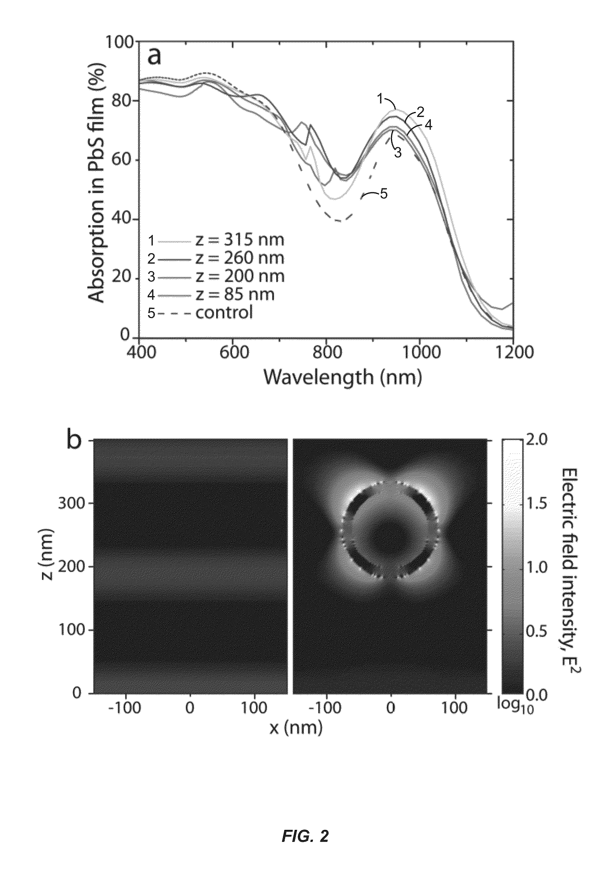
[0168]The devices were analyzed with full-wave finite-difference time-domain (FDTD) simulations to evaluate the potential impact of incorporating different types of metal nanoparticles into excitonically-tuned solar cells.
[0169]This example is suitable for candidate particles that are (1) compatibility with solution processing; (2) have a size range of less than ˜150 nm for integration in films with thicknesses of less than ˜400 nm; (3) have localized surface plasmon resonances (LSPRs) tunable to the near-IR (NIR) portion of the solar spectrum; or (4) scattering-to-absorption ratios (S) of greater than 1. In some instances, the candidate particles ha...
example 2
Nanoshells
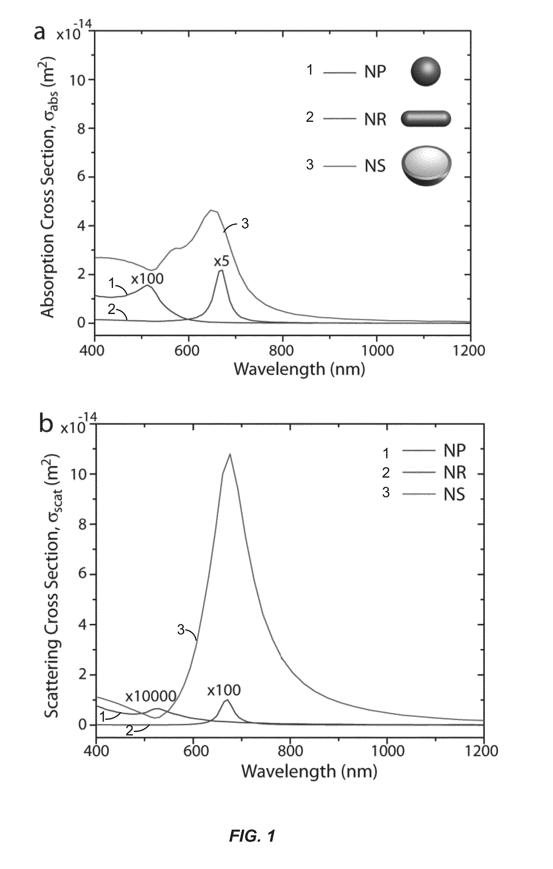
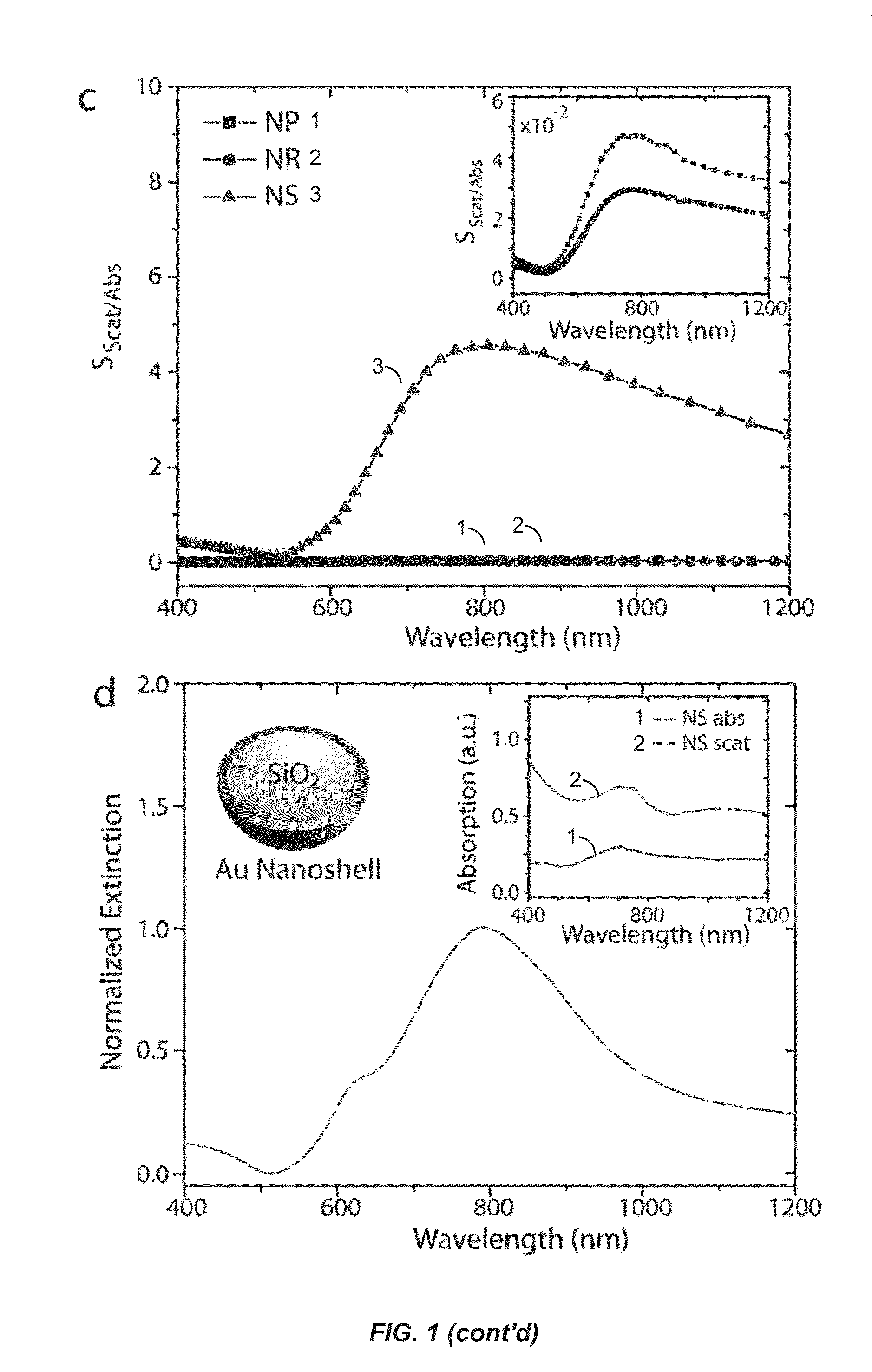
[0174]This example analyzes spherical dielectric-metal core-shell nanoparticles, a.k.a. nanoshells. FIG. 1d shows the measured extinction spectrum of nanoshells in methanol solution with a LSPR centered at 800 nm with a full-width at half-maximum of 280 nm. The extinction (absorption+near- and far-field scattering) cross-section is 3-5 orders of magnitude larger than that of either spherical nanoparticles or nanorods (FIG. 1a,b). Due to the presence of a thin metallic shell (˜15 nm), the optical interaction volume of these particles is therefore much larger. This in turn reduces the areal density required to scatter incident light completely while minimizing absorption. The theoretical S factor reaches its maximum at 4.5, and is larger than 3 over a wide spectral range in the near-infrared region (FIG. 1c). Additional calculations for large nanorods (66 nm in diameter and 512 nm in length), spherical nanoparticles (150 nm in diameter), and spherical dielectric particles (1...
example 3
Nanoshell Scattering Factor
[0177]This Example verifies S>1 for nanoshells by experimentally measuring the relative scattering and absorption contributions. A thin layer of nanoshells was deposited by drop-casting from the solution-phase onto a glass slide and separated the absorption and scattering components using integrating sphere spectrophotometry (see Methods below). FIG. 1d inset shows that, in the solid state, S is at least 2 over all wavelengths of interest (e.g., 400-1200 nm). In contrast, the S of nanorods deposited by a similar method was measured to be much less than 1 over the same wavelength range (FIG. 5).
[0178]FIG. 5 shows the UV-Vis-NIR absorption and scattering spectra taken in an integrating sphere for a drop-cast ensemble of (a) nanorods and (b) nanoshells on an ITO-coated glass substrate.
[0179]In FIG. 5, absorption (1) was measured by tilting the sample at a slight angle relative to the illumination beam with all other ports closed so that all directly transmitt...
PUM
 Abstract
Description
Claims
Application Information


