Gallium Nitride Substrates and Functional Devices

a technology of gallium nitride and substrate, applied in the direction of polycrystalline material growth, crystal growth process, chemically reactive gas, etc., can solve the problem of the limit of achieve the effect of reducing the actual obtained luminous intensity and superior uniformity of microstructur

Active Publication Date: 2016-02-18
NGK INSULATORS LTD
View PDF9 Cites 11 Cited by
  • Summary
  • Abstract
  • Description
  • Claims
  • Application Information

AI Technical Summary

Benefits of technology

[0012]The present inventors studied the case that the luminous intensities was lowered, when deviation photoluminescence peak intensities on a surface of a gallium nitride substrate is reduced to obtain a uniform gallium nitride substrate and a light emitting device structure is formed thereon. That is, in the case that the microstructure of the surface of such gallium nitride substrate was observed by cathode luminescence, it was proved that the deviation of cathode luminescence peak intensities was small and the uniformity of the microstructure was superior.
[0013]The inventors further studied for preventing the local concentration of the defects in such gallium nitride substrate, and found that it was rather effective to provide deviation in the cathode luminescence peak intensities on the surface of the gallium nitride substrate.

Problems solved by technology

However, as such gallium nitride substrate was produced and a light emitting structure is formed thereon, its luminous intensity actually obtained has a limit.
That is, even in the case that the deviation of the peak intensities of photoluminescence on the surface of the gallium nitride substrate is reduced, it is proved that it does not necessarily mean the improvement of function of a functional device such as the light emitting device or the like and there is a limit.

Method used


Image

  • Gallium Nitride Substrates and Functional Devices
  • Gallium Nitride Substrates and Functional Devices
  • Gallium Nitride Substrates and Functional Devices

Examples


example 1

[0087]The GaN substrate was produced according to the following procedure.

[0088]Specifically, it was prepared a self-supporting type seed crystal substrate 1 made of gallium nitride seed crystal whose in-plane distribution of dislocation density by CL (cathode luminescence) was 2×10⁸ / cm2 in average excluding its outer periphery of 1 cm.

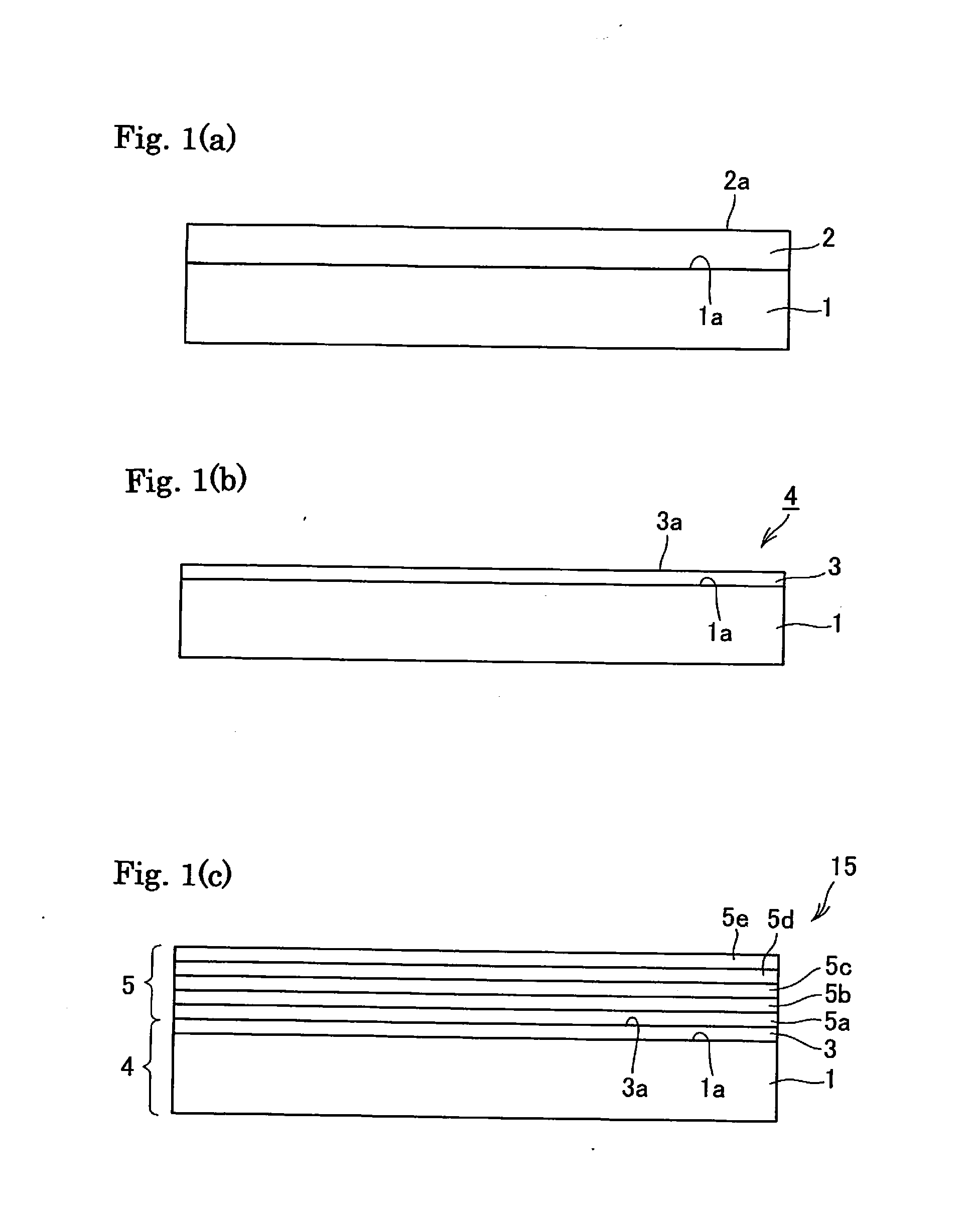
[0089]The gallium nitride substrate 1 was used to form a gallium nitride layer 2 by flux method. Specifically, Na and Ga were charged into a crucible, held at 870° C. and 4.0 MPa (nitrogen atmosphere) for 5 hours. Under such temperature and pressure conditions, it was proved that the supersaturation degree was low and the growth rate was very low as 0.5 μm / hr. Although it was grown about 2.5 μm after holding for 5 hours, the nuclei were rarely observed as described above and there were regions in part where the growth was hardly observed. Then, it was cooled to 850° C. for 10 minutes. Then, it was held at 4.0 MPa for 20 hours to grow the gallium nitri...

example 2

[0100]The experiment was carried out as the example 1, except that the frequency of the inversion of the rotational direction for agitating solution was made 400 seconds. It was thus obtained a colorless and transparent crystal 4 having a growth thickness of 200 μm. The average growth rate was about 10 μm / hr. An inclusion-containing layer was observed in a region of about 15 μm in the initial stage of growth. On the other hand, inclusions were not observed on the surface of the grown crystal. For the reference, FIG. 5 shows a fluorescence microscopic image of a gallium nitride layer by liquid phase process at a thickness of 200 μm.

[0101]The surface of the thus obtained gallium nitride layer of liquid phase process was subjected to CMP polishing until the thickness became 50 μm, and thereafter, the in-plane distribution of the dislocation density was measured by CL to prove to be 4 to 5×10⁶ / cm2. FIG. 6 shows an example of the CL image. It was observed a plurality of bright regions em...

example 3

[0104]The experiment was carried out as the example 1, except that the frequency of the inversion of the rotational direction for agitating solution was made 300 seconds. It was thus obtained a colorless and transparent crystal 2 having a growth thickness of 160 μm. The average growth rate was about 8 μm / hr. An inclusion-containing layer was observed in a region of about 15 μm in the initial stage of growth. On the other hand, inclusions were not observed on the surface of the grown crystal.

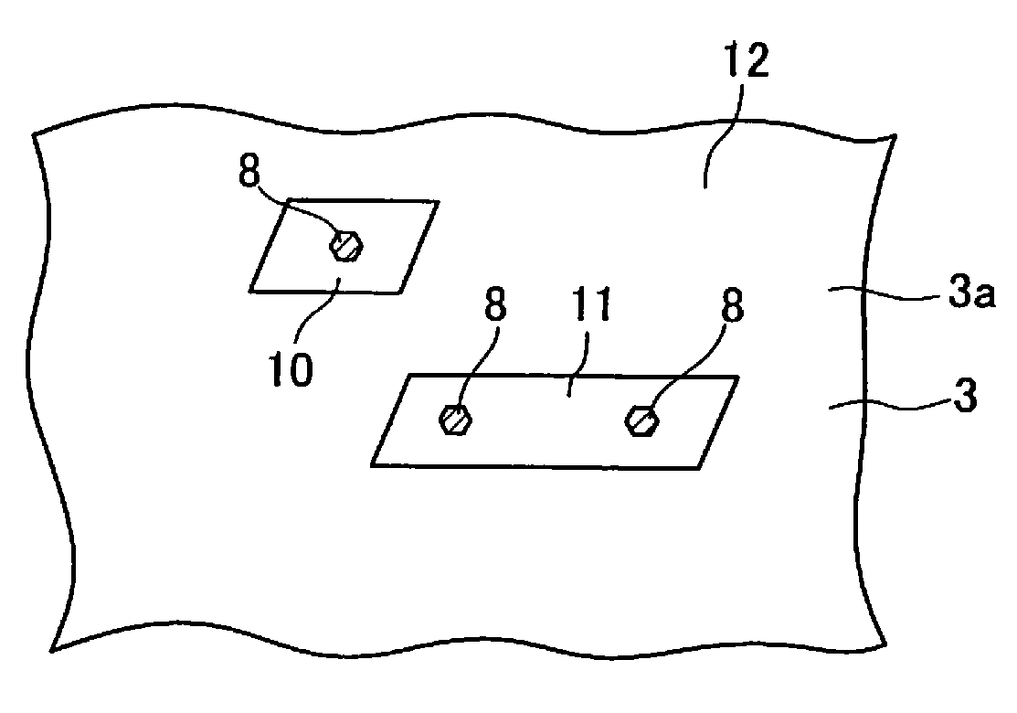
[0105]The surface of the thus obtained gallium nitride layer 2 of liquid phase process was subjected to CMP polishing until the thickness became 50 μm, and thereafter the in-plane distribution of the dislocation density was measured by CL to prove to be 4 to 5×10⁶ / cm2. FIG. 7 shows an example of the CL image. It was observed a plurality of bright regions emitting light in the observed visual field. The outline of the region had a shape substantially of a hexagonal or a parallelogram, as can be se...


PUM

PropertyMeasurementUnit
widthaaaaaaaaaa
length×0aaaaaaaaaa
widthaaaaaaaaaa

Abstract

The maximum value of peak intensities of cathode luminescence of a wavelength corresponding to a band gap of gallium nitride and in a measured visual field of 0.1 mm×0.1 mm is 140 percent or higher of an average value of the peak intensities of the cathode luminescence, provided that the peak intensities of the cathode luminescence are measured on a surface of the gallium nitride substrate.

Description

TECHNICAL FIELD[0001]The present invention relates to a gallium nitride substrate and a functional device.RELATED ART STATEMENT[0002]Recently, it has been extensively studied to use a nitride of a group 13 element, such as gallium nitride, to produce a semiconductor device such as a blue light LED, white light LED, blue-violet semiconductor laser or the like and to apply such semiconductor device to various kinds of electronic appliances.[0003]Flux method is a kind of liquid phase process. In the case of gallium nitride, by using sodium metal as flux, it is possible to reduce a temperature and pressure required for crystal growth of gallium nitride to about 800° C. and several MPa, respectively. Specifically, nitrogen gas is dissolved into mixed melt of sodium metal and gallium metal, so that gallium nitride becomes supersaturation state and grows as a crystal. According to such liquid phase process, dislocations are reduced than that in the case of vapor phase process, so that it i...

Claims


Application Information

Patent Timeline
Patent Type & Authority Applications(United States)
IPC IPC(8): H01L33/32H01L33/20
CPCH01L33/20H01L33/32C30B9/10C30B19/02C30B25/02C30B29/406H01L33/02
Inventor IWAI, MAKOTOSAKAI, MASAHIROIMAI, KATSUHIROKURAOKA, YOSHITAKA
Owner NGK INSULATORS LTD
Why Eureka
Try Eureka