

High power impulse magnetron sputtering process to achieve a high density high sp3 containing layer
a magnetron sputtering and high density technology, applied in the direction of vacuum evaporation coating, chemical vapor deposition coating, coating, etc., can solve the problems of high aspect ratio etching, limited reduction, and high cos
- Summary
- Abstract
- Description
- Claims
- Application Information
AI Technical Summary
Benefits of technology
Problems solved by technology
Method used
Image

Examples
Embodiment Construction
[0023]Embodiments disclosed herein generally relate to a nanocrystalline diamond layer formed on a substrate. Nanocrystalline diamond layers formed by the processes described herein generally have a higher mass density, higher etch selectivity, lower stress and excellent thermal conductivity needed for forming integrated circuit (IC) devices having small feature sizes. Embodiments are more clearly described with reference to the figures below.
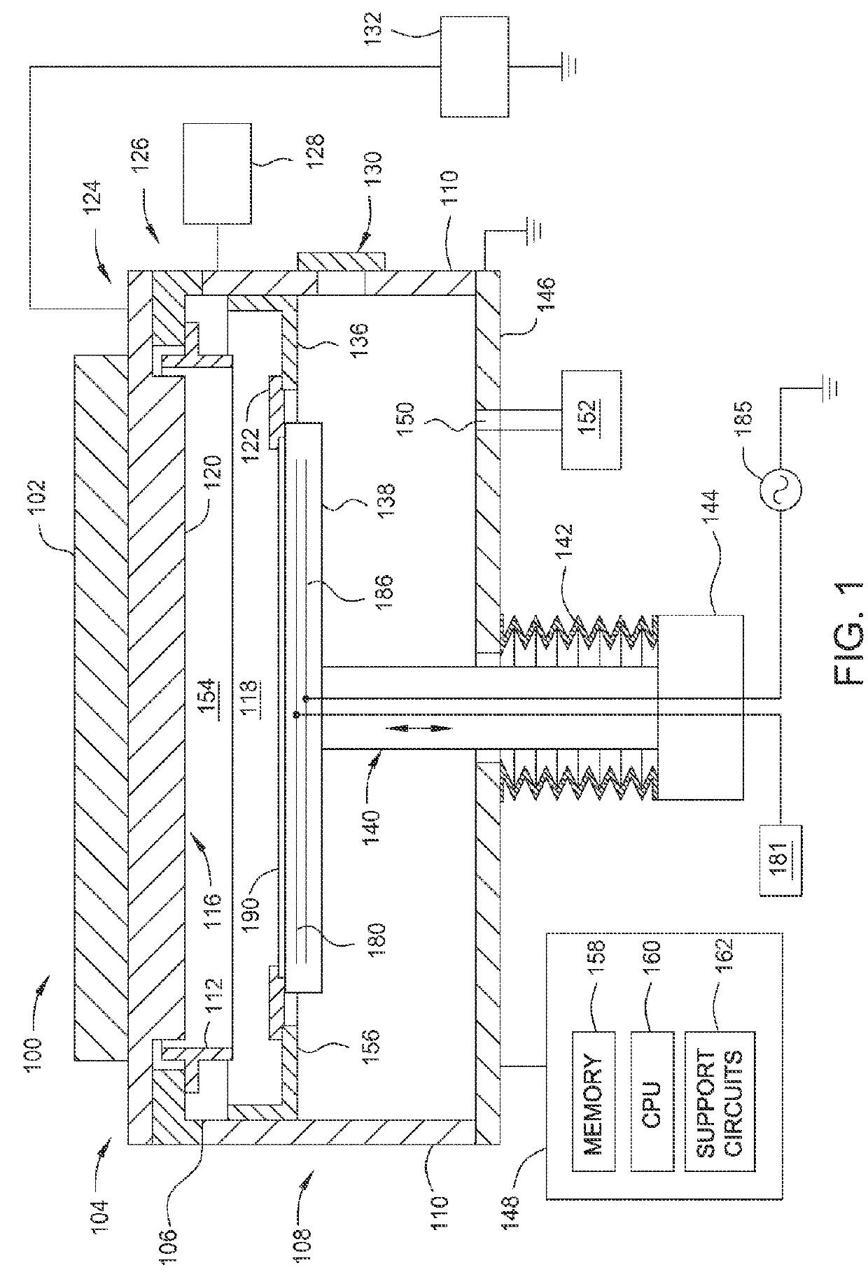
[0024]FIG. 1 illustrates an exemplary physical vapor deposition (PVD) process chamber 100 (e.g., a sputter process chamber) suitable for sputter depositing materials using a high power impulse magnetron sputtering (HIPIMS) process. One example of the process chamber that may be adapted to form the nanocrystalline diamond layer is a PVD process chamber, available from Applied Materials, Inc., located in Santa Clara, Calif. It is contemplated that other sputter process chambers, including those from other manufactures, may be adapted to practice ...
PUM
| Property | Measurement | Unit |
|---|---|---|
| pressure | aaaaa | aaaaa |
| pressure | aaaaa | aaaaa |
| temperature | aaaaa | aaaaa |
Abstract
Description
Claims
Application Information