Organic light-emitting diode, array substrate and preparation method thereof, and display device

a light-emitting diode and organic technology, applied in the field of display technology, can solve the problems of color offset, unfavorable display field at the level of pixels, many problems to be improved, etc., and achieve the effect of improving the external quantum simplifying the preparation process, and enhancing the light extraction efficiency of the organic light-emitting diod

Active Publication Date: 2016-05-05
BOE TECH GRP CO LTD
View PDF6 Cites 19 Cited by
  • Summary
  • Abstract
  • Description
  • Claims
  • Application Information

AI Technical Summary

Benefits of technology

[0035]In the organic light-emitting diode of the present invention, by doping metal nanoparticles in the hole injection layer and allowing the frequency of localized surface plasmon resonance of the metal nanoparticles to be matched with the emission wavelength of the light-emitting layer, the metal nanoparticles and photons emitted from the light-emitting layer are allowed to generate localized surface plasmon resonance, so that the external quantum efficiency of the organic light-emitting diode is improved, the light extraction efficiency of the organic light-emitting diode is enhanced, the light extraction efficiency of the array substrate is thus enhanced, and the display effect of the display device is further ensured; meanwhile, the formation of the hole injection layer in an inkjet printing manner is simple and practical, simplifies preparation process and improves preparation efficiency.

Problems solved by technology

However, many problems remain to be improved at present, in which how to improve the light extraction efficiency of the OLED is still one of key points.
However, the micro lens generally only can realize the improvement of the light extraction efficiency in the illumination field, but is still not beneficial in the display field at the level of pixels having fine size.
The use of the micro-cavity structure generally will result in the deviation of the outgoing light color of the OLED and a narrower angle of view, and the photonic crystal requires a complicated photo-etching process, is difficult to be prepared and realized, and meanwhile may further cause color offset and other problems of view angle due to the presence of optical gratings and the like.
The Bragg diffraction technology generally requires that emergent light is adjusted by alternately laminating multiple layers of materials having high and low refractivity with thicknesses of high precision; meanwhile, different light-emitting colors (such as red R, green G and blue B) require different best thicknesses of Bragg diffraction layers, so the precise adjustment of the thicknesses of RGB must be realized by multiple steps of depositions, mask exposures and etching processes, which has large difficulty, low yield and high cost for the preparation technology of full-color OLED display devices.

Method used


Image

  • Organic light-emitting diode, array substrate and preparation method thereof, and display device
  • Organic light-emitting diode, array substrate and preparation method thereof, and display device
  • Organic light-emitting diode, array substrate and preparation method thereof, and display device

Examples


embodiment 1

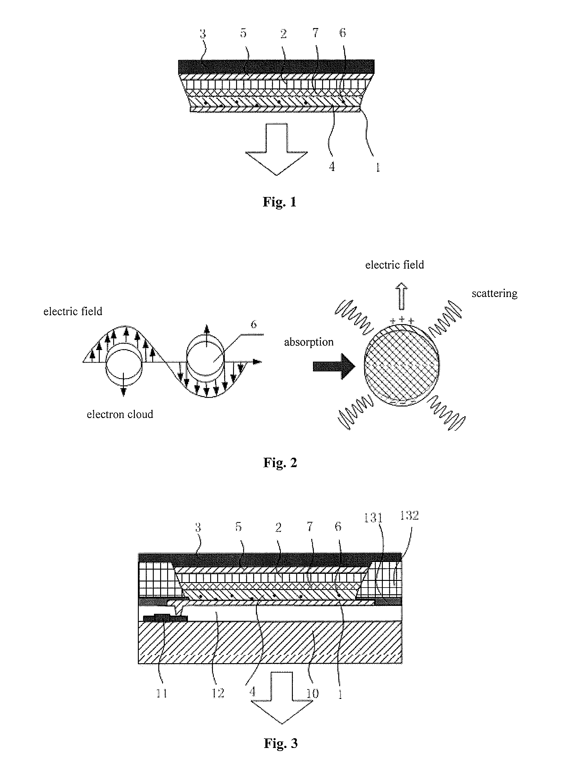
[0045]Referring to FIG. 1, this embodiment provides an organic light-emitting diode. The organic light-emitting diode includes an anode 1, a cathode 3, a light-emitting layer 2 disposed between the anode 1 and the cathode 3, and a Hole Injection Layer (HIL) 4 disposed between the anode 1 and the light-emitting layer 2, the hole injection layer 4 is provided therein with metal nanoparticles 6, wherein the frequency of localized surface plasmon resonance of the metal nanoparticles 6 is matched with the emission wavelength of the light-emitting layer 2.

[0046]The metal nanoparticles 6 are generally made from inert noble metals, for example, any one of gold, silver and aluminum, or an alloy of gold, silver and aluminum, or any combination of gold, silver and aluminum. The shape of the metal nanoparticles 6 is any one or any combination of a spherical shape, a prismatic shape, a cubic shape, a cage shape and a core-shell structure.

[0047]Preferably, the range of particle size of the metal ...

embodiment 2

[0095]This embodiment provides an OLED. The difference between this embodiment and Embodiment 1 lies in that the hole injection layer of the OLED in this embodiment has more than one sub-layers. For example, the hole injection layer includes a first hole injection sub-layer and a second hole injection sub-layer.

[0096]In this embodiment, the hole injection layer includes a first hole injection sub-layer and a second hole injection sub-layer. The metal nanoparticles are disposed in the first hole injection sub-layer, and the second hole injection sub-layer is closer to the light-emitting layer than the first hole injection sub-layer.

[0097]In this embodiment, the structure of the hole injection layer in the OLED is fine-adjusted locally, mainly involving the adjustment of a distance from the metal nanoparticles to a recombination luminescent region of excitons. In other words, the first hole injection sub-layer with metal nanoparticles embedded therein may be first formed by inkjet pri...

embodiment 3

[0100]This embodiment provides an array substrate, including the OLED of Embodiment 1 or Embodiment 2.

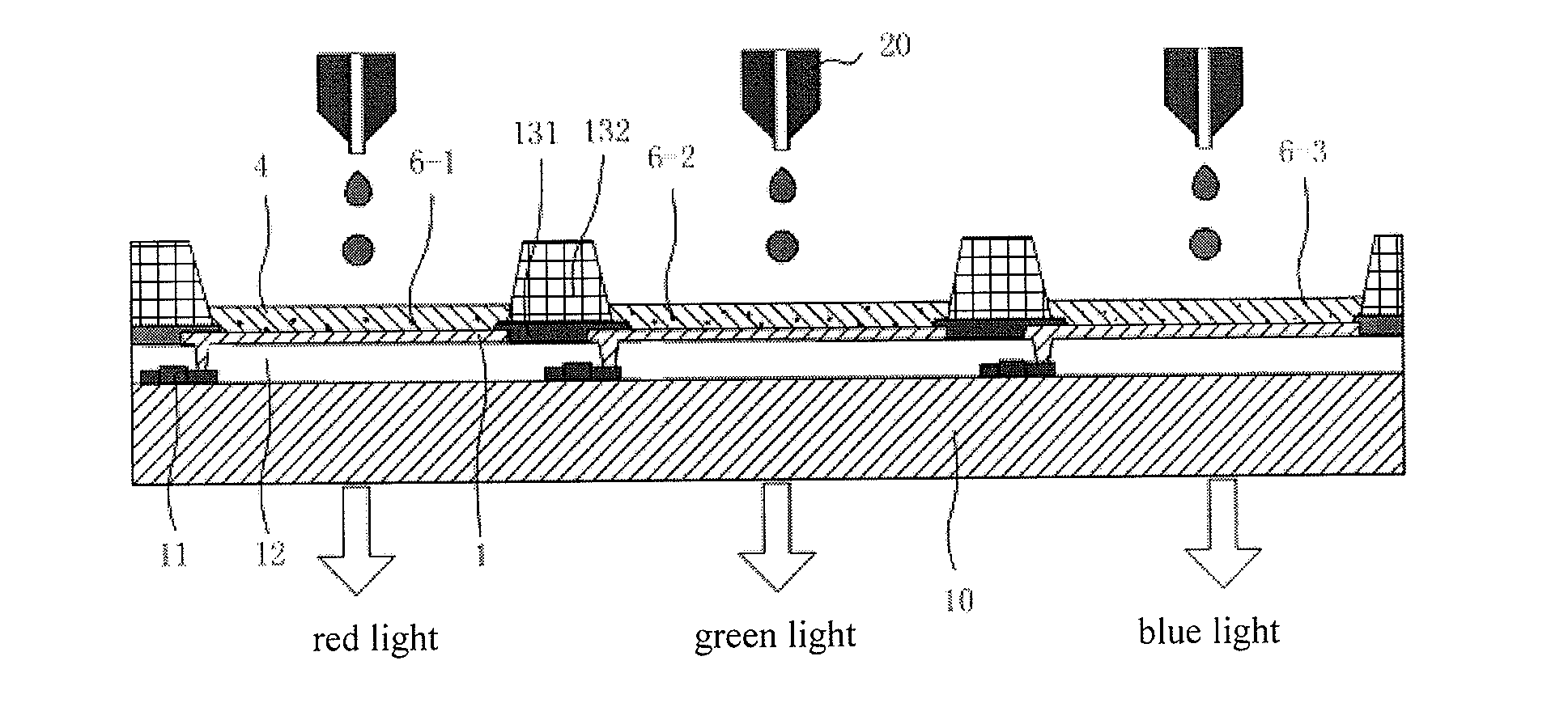
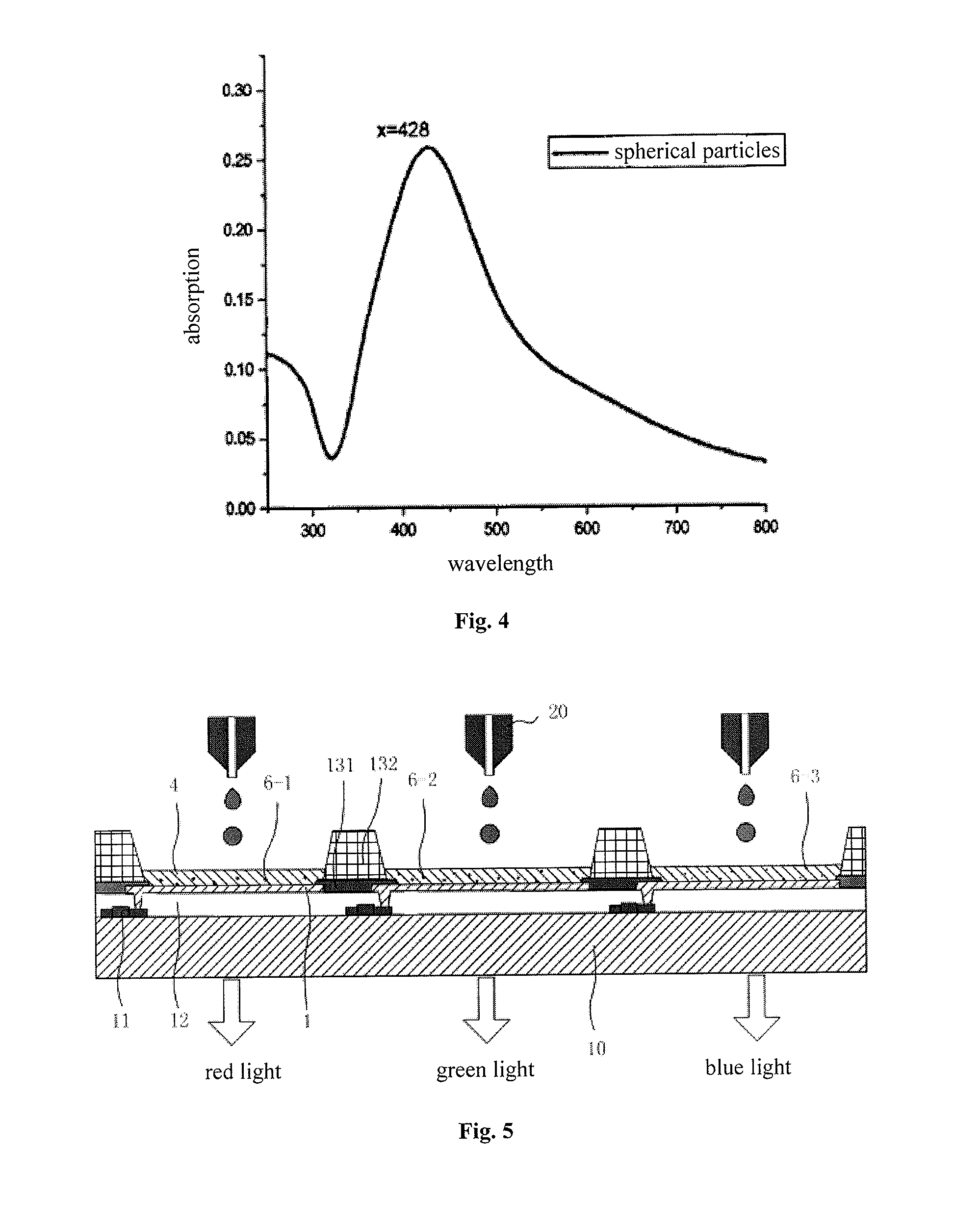
[0101]As shown in FIG. 5, the array substrate is divided into a plurality of sub-pixel regions. Each of the sub-pixel regions is provided therein with an organic light-emitting diode. The array substrate includes a red organic light-emitting diode, a green organic light-emitting diode and a blue organic light-emitting diode, the red organic light-emitting diode, the green organic light-emitting diode and the blue organic light-emitting diode being successively disposed in three adjacent sub-pixel regions, respectively.

[0102]In this embodiment, each of the sub-pixel regions is further provided therein with a Thin Film Transistor (TFT) for driving the organic light-emitting diode, the drain of the thin film transistor is connected to the anode of the organic light-emitting diode. FIG. 5 shows a structure of a common array substrate, having an active drive OLED, containing thin film tr...


PUM

PropertyMeasurementUnit
particle sizeaaaaaaaaaa
internal quantum efficiencyaaaaaaaaaa
coupling light extraction efficiencyaaaaaaaaaa

Abstract

The present invention relates to an organic light-emitting diode, an array substrate and a preparation method thereof, and a display device. The organic light-emitting diode comprises an anode, a cathode, a light-emitting layer disposed between the anode and the cathode, and a hole injection layer disposed between the anode and the light-emitting layer, wherein the hole injection layer is provided therein with metal nanoparticles, and the frequency of a localized surface plasmon resonance of the metal nanoparticles is matched with the emission wavelength of the light-emitting layer. As the organic light-emitting diode is doped with metal nanoparticles in the hole injection layer and the resonance frequency of the localized surface plasmon of the metal nanoparticles is matched with the emission wavelength of the light-emitting layer, the metal nanoparticles are allowed to generate localized plasma resonance with photons, so that the light extraction efficiency of the organic light-emitting diode is enhanced.

Description

FIELD OF THE INVENTION[0001]The present invention belongs to the field of display technology, and particularly relates to an organic light-emitting diode, an array substrate and a preparation method thereof, and a display device.BACKGROUND OF THE INVENTION[0002]Organic Light-Emitting Diodes (OLEDs) are honored as a new generation of flat panel displays. In comparison to current mainstream Liquid Crystal Displays (LCDs), the organic light-emitting diodes have the advantages of self illumination, wide angle of view, high contrast ratio, short response time, thin panel thickness (flattening), flexible display and the like. The basic structure of an organic light-emitting diode comprises an anode, a cathode and a light-emitting layer between the anode layer and the cathode layer. Under the action of an external voltage, electrons and holes are injected from the cathode and the anode respectively, then are transferred and encounter with each other in the light-emitting layer to generate ...

Claims


Application Information

Patent Timeline
Patent Type & Authority Applications(United States)
IPC IPC(8): H01L51/52H01L51/00H01L51/56H01L51/50H01L27/32
CPCH01L51/5262H01L51/5088H01L27/3211H01L2227/323H01L51/56H01L51/0004H01L2251/301H01L27/3248H10K59/125H10K71/13H10K59/122H10K50/17H10K50/85H10K71/135H10K59/12H10K50/15H10K2102/331H10K59/35H10K59/123H10K71/00H10K59/1201H10K2102/00
Inventor DAI, QINGHOU, WENJUNLIU, ZE
Owner BOE TECH GRP CO LTD
Why Eureka
Try Eureka