Nanostructured photocatalysts and doped wide-bandgap semiconductors

a photocatalyst and nanostructure technology, applied in the field of nanostructured photocatalysts and semiconductors, can solve the problems of preventing rational design of new photocatalysts with higher efficiency and/or selectivity, affecting the observation of high photocatalytic activity and selectivity, and affecting the effect of chemical modification on the electronic structure of tiosub>2 /sub>semiconductor, etc., to achieve the effect o

Active Publication Date: 2016-07-07
UNIV OF COLORADO THE REGENTS OF
View PDF7 Cites 27 Cited by
  • Summary
  • Abstract
  • Description
  • Claims
  • Application Information

AI Technical Summary

Benefits of technology

[0011]Cadmium Sulfide (CdS) nanostructures (e.g., different-sized nanoparticles, nanorods, metal-hybrid nanostructures, and core-shell nanostructures) are designed herein to improve various photophysical steps leading to formation of desired solar fuels. In particular, CdS nanoparticles with 3.07 eV bandgap, well matched with the reduction potential of aldehydes, show an increased photocatalytic activity (˜40% external quantum yield) and selectivity (>99%) for acetaldehyde production.

Problems solved by technology

While modified TiO2-based photocatalysts can be used for water splitting or CO2-water reduction, the effect of chemical modification on the electronic structure of TiO2 semiconductor is largely unexplored.
Moreover, lack of insight into photophysics governing recombination pathways, defect mediated photocatalytic reduction, and energetic levels participating in electronic reduction of CO2 following photogeneration of electron-hole pair has also prevented rational design of new photocatalysts with higher efficiency and / or selectivity.
However, lack of suitable energetic states, charge conduction pathways, light harvesting, or interfacial charge trapping / recombination impedes observation of high photocatalytic activity and selectivity in multielectron reduction of CO2 and H2O.
Most applications are focused on bulk semiconductor films, since doping semiconductor nanostructures has proven challenging.
This can severely limit their applications and device architectures, like fabricating p-type oxide films or changing the doping level of n-type dopant for optimized configuration.
Moreover, addition of desired dopants, like shallow or deep donors, can also lead to formation of heavily-doped transparent oxide nanostructures, or co-doped photocatalysts which can absorb infrared light.
While photocatalytic reduction of carbon dioxide (CO2) into solar fuels can provide an alternative, lack of insight into energetic pathways governing photocatalysts has impeded study.
While easy incorporation of dopants can be achieved in bulk semiconductors, doping semiconductor nanostructures has proven difficult.
Increase in sunlight illumination results in change in product yields due to filling up of lower energy levels and likely slower cooling of hot carriers, resulting in products with higher reduction potentials.
(B) TiO2—Cu2-xO photocatalyst shows higher yields (internal quantum efficiency (QE)) for CO2-water reduction than unmodified TiO2, but variation in oxidation state of copper results in change in semiconductor bandgap (see FIG. 7) and traps on the surface, leading to enhanced recombination, lower yields and unselective product formation.
The dashed-black line represents the large Rayleigh scattering observed in these nanotubes, which makes exact determination of bandgaps difficult in these indirect bandgap semiconductors, using optical spectroscopy.

Method used


Image

  • Nanostructured photocatalysts and doped wide-bandgap semiconductors
  • Nanostructured photocatalysts and doped wide-bandgap semiconductors
  • Nanostructured photocatalysts and doped wide-bandgap semiconductors

Examples


Embodiment Construction

[0065]The following description of technology is merely exemplary in nature of the subject matter, manufacture and use of one or more inventions, and is not intended to limit the scope, application, or uses of any specific invention claimed in this application or in such other applications as may be filed claiming priority to this application, or patents issuing therefrom. Regarding the methods disclosed, the order of the steps presented is exemplary in nature, and thus, the order of the steps can be different in various embodiments. Except in the examples, or where otherwise expressly indicated, all numerical quantities in this description, including amounts of material or conditions of reaction and / or use, are to be understood as modified by the word “about” in describing the broadest scope of the technology.

[0066]Photocatalyst for Carbon Dioxide-Water Reduction

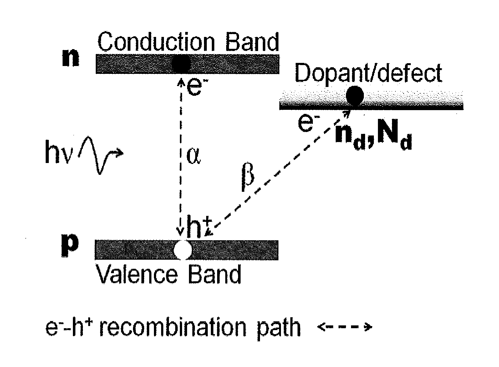
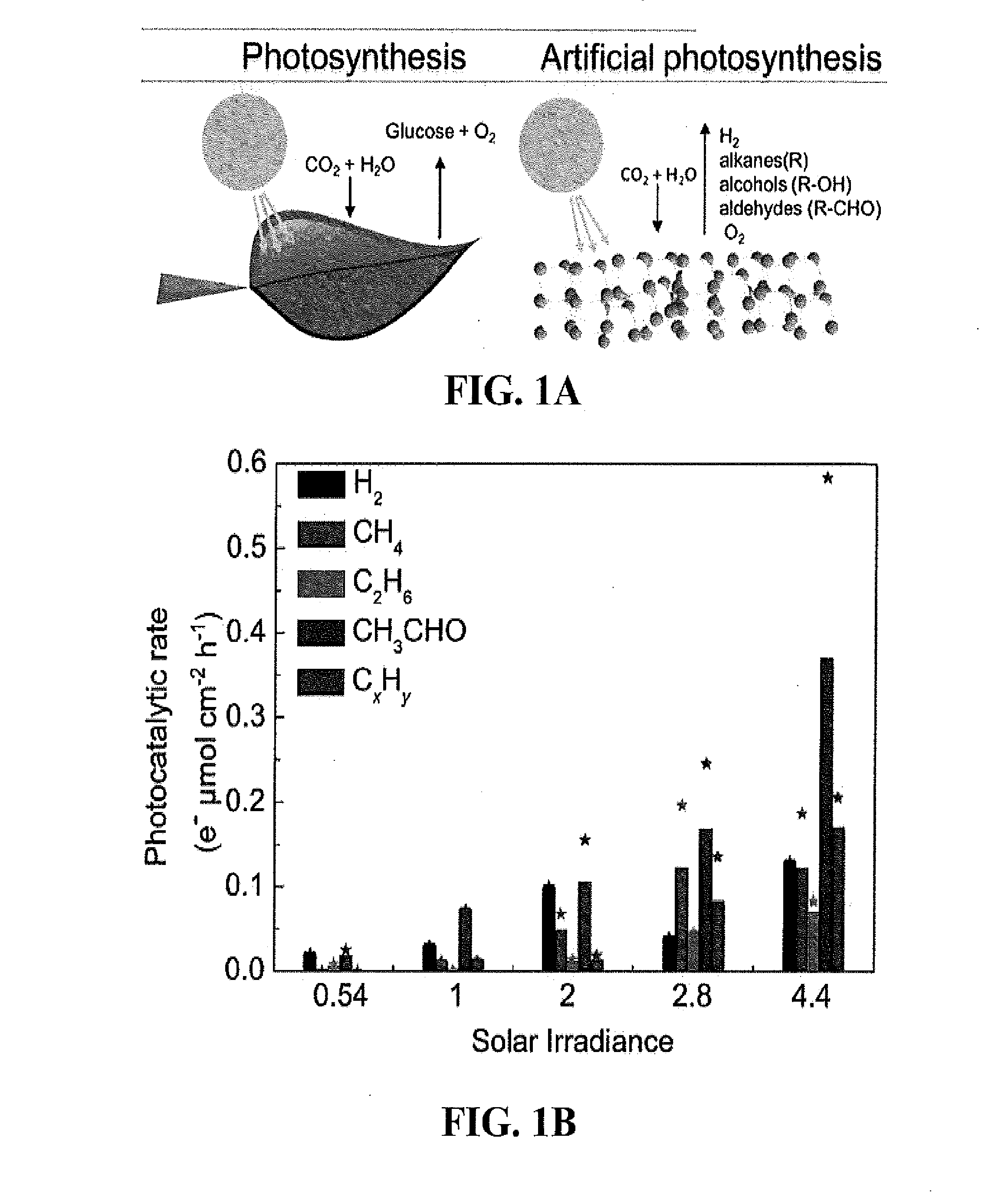
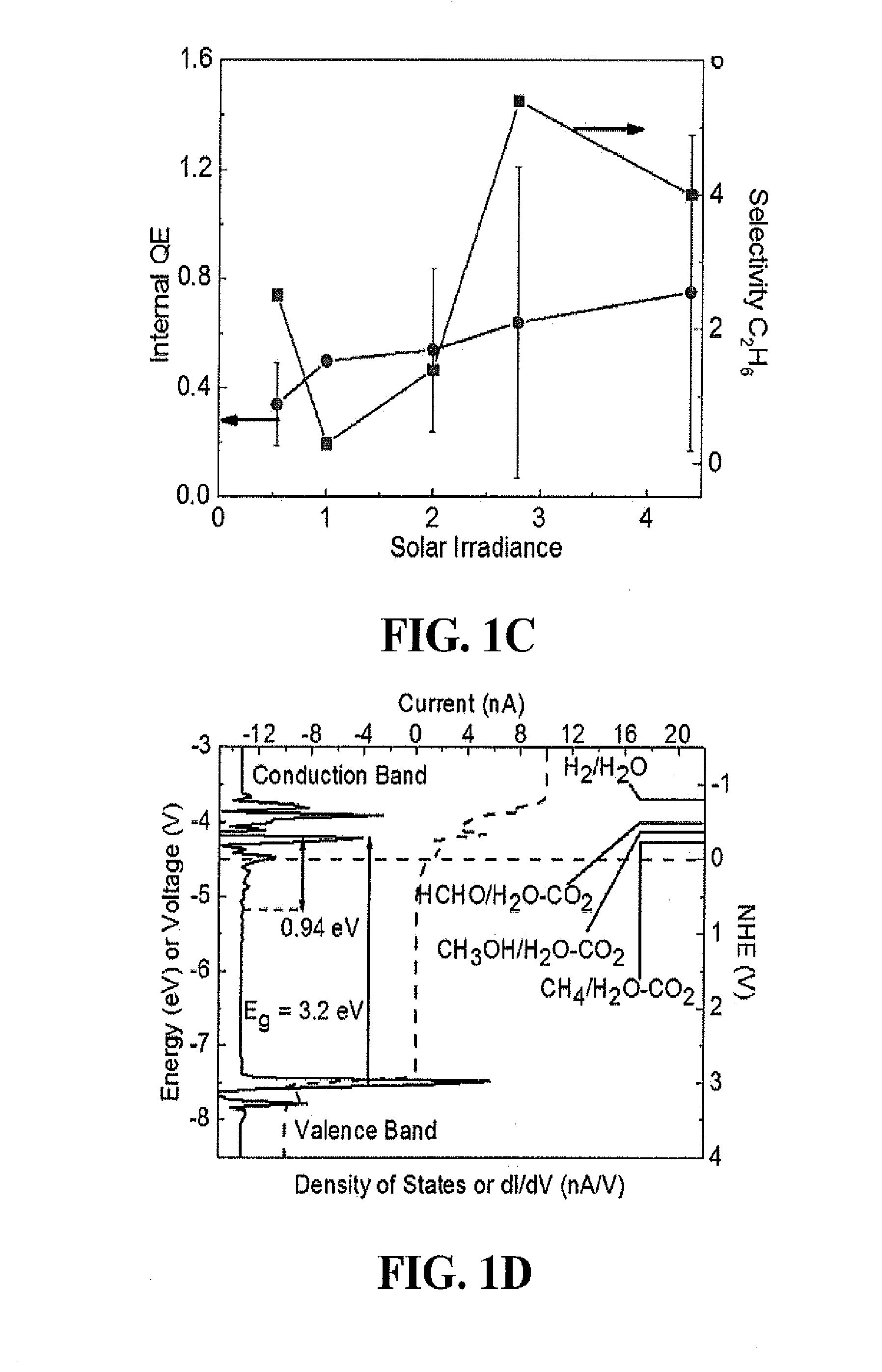
[0067]Titanium dioxide (TiO2) has been extensively studied for several photocatalysis, photoelectrochemical, and catalyti...


PUM

PropertyMeasurementUnit
diameteraaaaaaaaaa
diameteraaaaaaaaaa
diameteraaaaaaaaaa

Abstract

Photocatalysts for reduction of carbon dioxide and water are provided that can be tuned to produce certain reaction products, including hydrogen, alcohol, aldehyde, and/or hydrocarbon products. These photocatalysts can form artificial photosystems and can be incorporated into devices that reduce carbon dioxide and water for production of various fuels. Doped wide-bandgap semiconductor nanotubes are provided along with synthesis methods. A variety of optical, electronic and magnetic dopants (substitutional and interstitial, energetically shallow and deep) are incorporated into hollow nanotubes, ranging from a few dopants to heavily-doped semiconductors. The resulting wide-bandgap nanotubes, with desired electronic (p- or n-doped), optical (ultraviolet bandgap to infrared absorption in co-doped nanotubes), and magnetic (from paramagnetic to ferromagnetic) properties, can be used in photovoltaics, display technologies, photocatalysis, and spintronic applications.

Description

CROSS-REFERENCE TO RELATED APPLICATIONS[0001]This application claims the benefit of U.S. Provisional Application No. 61 / 841,510, filed on Jul. 1, 2013, and the benefit of U.S. Provisional Application No. 61 / 879,168, filed on Sep. 18, 2013. The entire disclosures of the above applications are incorporated herein by reference.GOVERNMENT RIGHTS[0002]This invention was made with U.S. Government support under CAREER CBET awarded by the National Science Foundation (NSF). The U.S. Government has certain rights in the invention.FIELD[0003]The present technology relates to nanostructured photocatalysts and semiconductors, including photosynthetic devices and doped wide-bandgap semiconductor nanotubes that are monodoped or co-doped.INTRODUCTION[0004]This section provides background information related to the present disclosure which is not necessarily prior art.[0005]Simultaneous reduction of CO2 and water using sunlight has been an important step in the life cycle on Earth. This single react...

Claims


Application Information

Patent Timeline
Patent Type & Authority Applications(United States)
IPC IPC(8): B01J35/00B01J27/04C01G11/02B01J27/057B01J35/02B01J23/72B01J27/051C25B3/25
CPCB01J35/004B01J23/72B01J27/04B01J27/051C01P2004/51B01J35/0013B01J35/023C01G11/02C01P2004/16B01J27/0573Y02P20/133C25B1/04B01J27/047Y02E60/36C25B3/25C25B11/091
Inventor NAGPAL, PRASHANTSINGH, VIVEKCASTELLANOS BELTRAN, IGNACIOALIVOV, YAHYADING, YUCHENCERKOVNIK, LOGAN JEROME
Owner UNIV OF COLORADO THE REGENTS OF
Why Eureka
Try Eureka