Host materials and ligands for dopants in organic light emitting diodes

a technology of organic light-emitting diodes and host materials, which is applied in the field of organic electronics, can solve the problems of low success rate, long time lines, and high cos

Active Publication Date: 2016-08-11
UNIV OF SOUTHERN CALIFORNIA
View PDF3 Cites 4 Cited by
  • Summary
  • Abstract
  • Description
  • Claims
  • Application Information

AI Technical Summary

Benefits of technology

[0013]The advent of high speed computers allows the researcher to query libraries for the properties of the compounds contained therein in a parallel fashion. Instead of waiting for serendipity to produce a new OLED material, an investigator can use the computer to assemble and query a library of potential OLED host materials to find the proverbial needles in a haystack. The reason for the serial approach used to date is that there was a significant amount of time needed to assay one material. It was impractical to investigate a large number of molecules in the lab or on the computer, so the researcher focused on the molecules that their intuition told them were the most likely compounds with desired properties. Using an electronically generated OLED host compound libra

Problems solved by technology

This process suffers from low success rates, long time lines, and high costs, particularly as the desired materials increase in complexity.
When a material is composed o

Method used


Image

  • Host materials and ligands for dopants in organic light emitting diodes
  • Host materials and ligands for dopants in organic light emitting diodes
  • Host materials and ligands for dopants in organic light emitting diodes

Examples


example 1

Experimental Section

Introduction

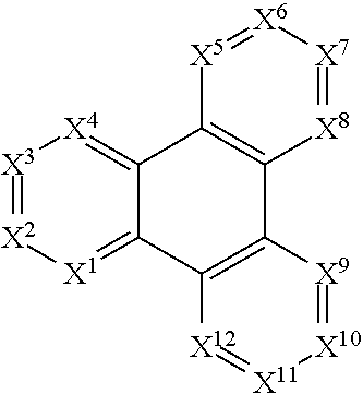
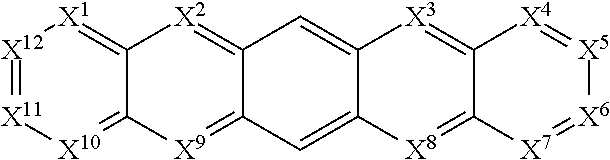
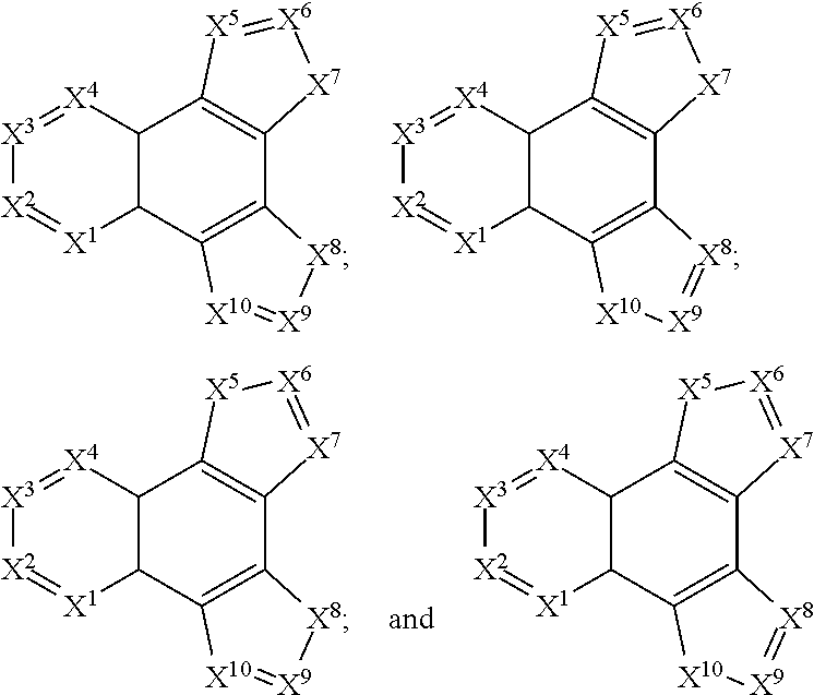
[0181]Due to synthetic accessibility, most reported H2P derivatives are based on 1,10-[f]phenanthroline. There is no report of H2Ps with potential high triplet energies with different nitrogen placement other than 1,10-positions. By placing nitrogen atoms at different position on H2P, physical properties such as triplet energy, redox potential, and charge transport ability can be tuned to meet the requirements of blue PhOLED applications. For example, three H2P isomers based on imidazo[4,5-f]-1,10-phenanthroline, imidazo[4,5-f]-3,8-phenanthroline, and imidazo[4,5-f]-4,7-phenanthroline derivative were shown to possess different triplet energies ranging from 2.76-2.91 eV. Moreover, significant discrepancies in their hole-transport properties lead to more than 10 times difference in device efficiencies for the H2P-based devices. Computations based on the methods of the invention for these H2P hosts not only showed triplet energies well-matched to the exp...

example 2

Screening Methods for OLED Materials

[0192]Once a library has been identified and the molecular modeling software has been used to predict the electronic properties of each member of that library, the library needs to be searched to find the optimal compounds for the chosen application, in the present case for use as host materials in phosphorescent OLEDs. In other embodiments, the library needs to be searched to find the optimal compounds for use as host materials in OLEDs which operate by one or more of phosphorescent, fluorescent, TADF, or triplet-triplet annihilation processes. The approach described here could be used for OLEDs of any color (e.g. blue). Exemplary screening methods include sorting the library by singlet, triplet, HOMO, LUMO energies as well as dipole moment and reorganization energies for holes and electrons and set thresholds for each, based on a given dopant. With sufficiently stringent thresholds only a small number of compounds in the library will meet all of...

example 3

Screening Libraries for OPV Materials

[0205]The basic mechanism of photocurrent generation in OPVs can be illustrated with two organic materials, one a net electron donor (D) and the other an acceptor (A). The process is illustrated in FIG. 14 and can be broken down into four sequential steps. The first step is light absorption, leading to exciton formation. The exciton can be formed in either the donor or acceptor layer. The exciton then diffuses to the D / A interface, or alternatively decays to the ground state. The optimal thickness is determined by the exciton diffusion length, which is related to the ratio of the diffusion rate, kdiff; to its natural decay rate, kdecay. The typically short exciton diffusion lengths (LD) of ˜10 nm limiting the thickness of D and A layers, and thus the amount of light that can be collected and ultimately the efficiency of OPVs.

[0206]At the D / A interface, the exciton undergoes a charge transfer reaction, forming a hole and electron in the D and A la...


PUM


Abstract

Compound libraries, systems, methods, and apparatus, including computer program apparatus, are described for implementing techniques for processing data from a combinatorial inquiry to determine materials of use in various photoelectronic devices, e.g., organic light emitting diodes. The libraries include a collection of putative compounds of use as components of OLED devices, which are cross-referenced with one or more electronic property relevant to the efficacy of the compounds in an OLED device. The techniques broadly include receiving data from a chemical experiment on a library of materials having a plurality of members and generating a queriable representation of the chemical experiment. The chemical experiment is optionally an in silico experiment.

Description

PRIORITY[0001]This application claims the benefit of U.S. Patent Application Nos. 61 / 897,091, filed Oct. 29, 2013, 62 / 036,533, filed Aug. 12, 2014, 62 / 003,472, filed May 27, 2014 and 61 / 994,065, filed May 15, 2014, all of which are expressly incorporated by reference in their entirety.BACKGROUND OF THE INVENTION[0002]The field of organic electronics is in a stage of explosive growth. Ten years ago there was a great deal of promise in optoelectronic devices based on organic materials and today they are a reality. Samsung is making 10 million Galaxy cell phones a month with organic LED displays. Samsung and LG are selling 55″, curved screen, high definition televisions, again composed solely of organic LEDs. Organic solar cells have been advanced to efficiencies exceeding amorphous silicon based devices and their current rate of increase will exceed thin film devices in five years and be competitive with crystalline silicon, the industry standard, on the horizon. Organic transistors h...

Claims


Application Information

Patent Timeline
IPC IPC(8): G06F17/50H01L51/50
CPCH01L51/5028G06F17/5036G06F2111/20G06F30/367H10K71/30H10K85/00H10K85/6572H10K85/657H10K50/11H10K2101/10H10K2101/30
Inventor THOMPSON, MARK E.SARIS, PATRICKDJUROVICH, PETER I.CHEN, HSIAO-FAN
Owner UNIV OF SOUTHERN CALIFORNIA
Why Eureka
Try Eureka