Thermal spreader having inter-metal diffusion barrier layer

a technology of diffusion barrier layer and thermal spreader, which is applied in the direction of semiconductor devices, lighting and heating apparatus, semiconductor device details, etc., can solve the problems of increasing the requirement of enhanced heat spreaders to remove the heat from the device, reducing increasing the risk of emerging materials or costly, so as to reduce the heat spreading within the device, the effect of high-performance thermal stack and high wafer packing density

Inactive Publication Date: 2016-09-22
RAYTHEON CO
View PDF3 Cites 8 Cited by
  • Summary
  • Abstract
  • Description
  • Claims
  • Application Information

AI Technical Summary

Benefits of technology

[0002]As is known in the art, heat spreaders are used to spread heat generated from a heat source, such as heat generated in an electrical circuit, and then thermally conduct the spread heat to a heat sink. As is also known in the art, in order to meet cost and performance goals, Monolithic Microwave Integrated Circuit (MMIC) devices are moving away from coplanar waveguide (CPW) designs to microstrip designs, allowing for higher wafer packing densities exacerbating the need for a high performance thermal stack. The MMIC devices having for example

Problems solved by technology

This thinning unfortunately diminishes heat spreading within the device so the requirement of enhanced heat spreaders to remove the heat from the device becomes greater as the dev

Method used


Image

  • Thermal spreader having inter-metal diffusion barrier layer
  • Thermal spreader having inter-metal diffusion barrier layer
  • Thermal spreader having inter-metal diffusion barrier layer

Examples


Embodiment Construction

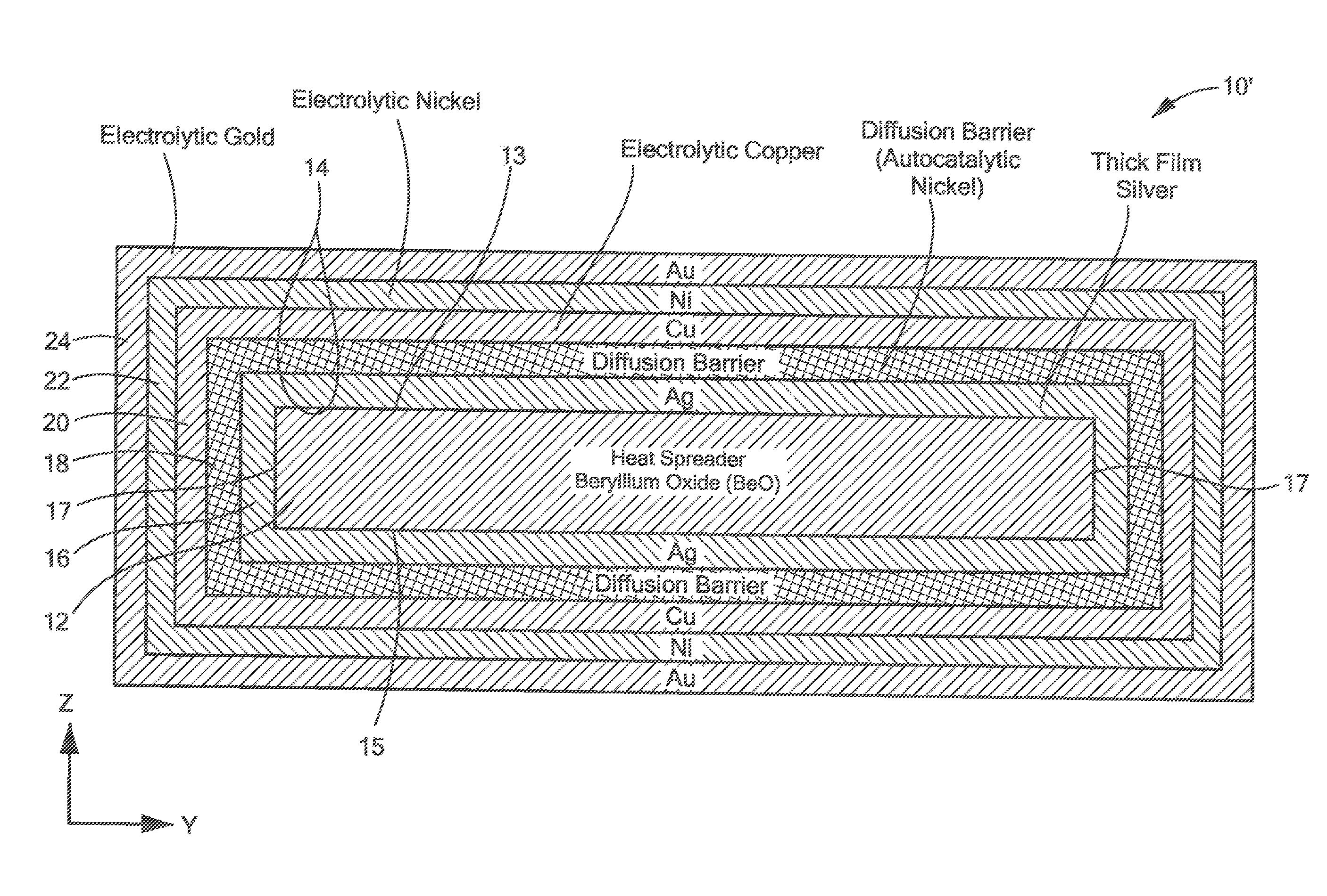
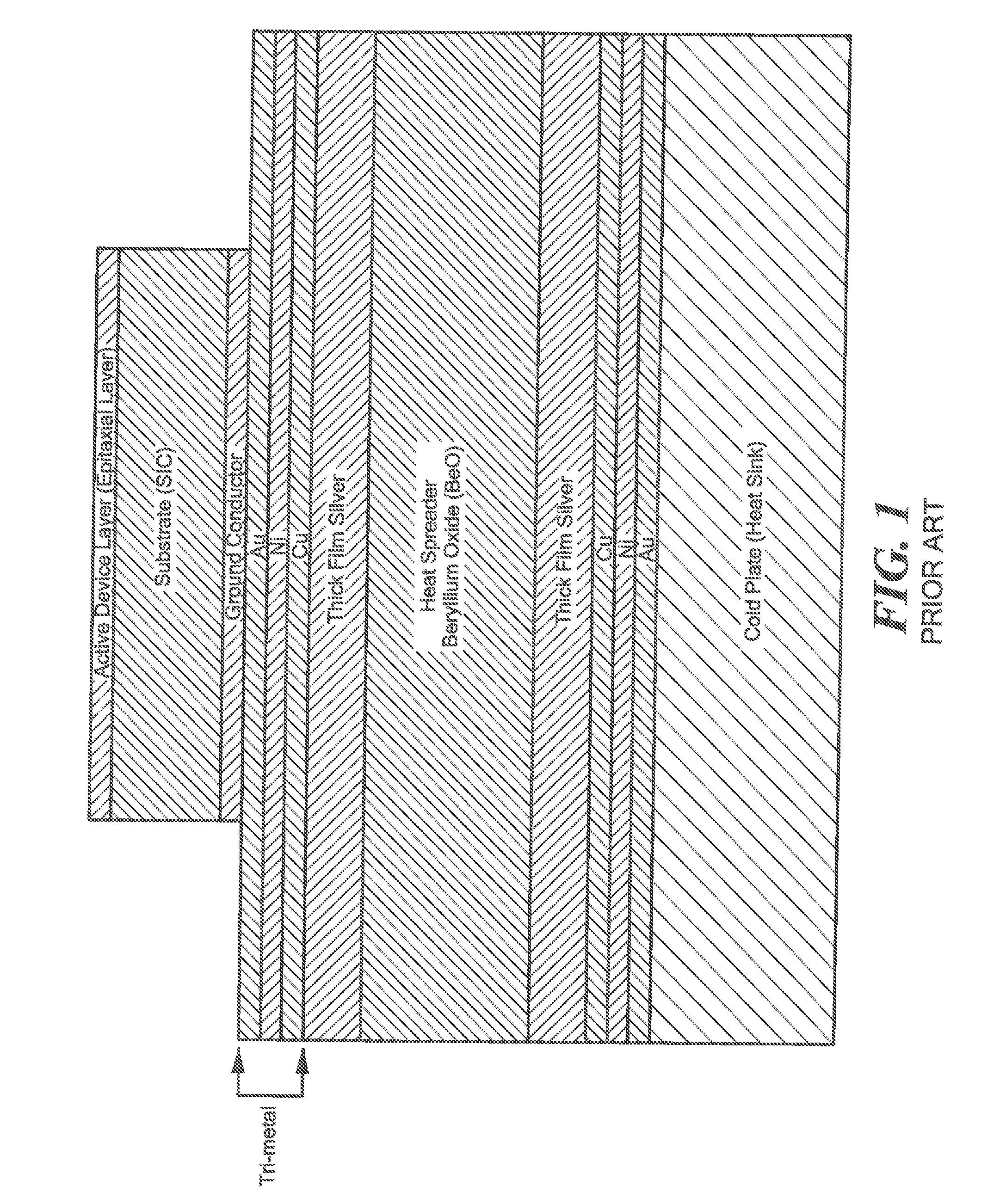
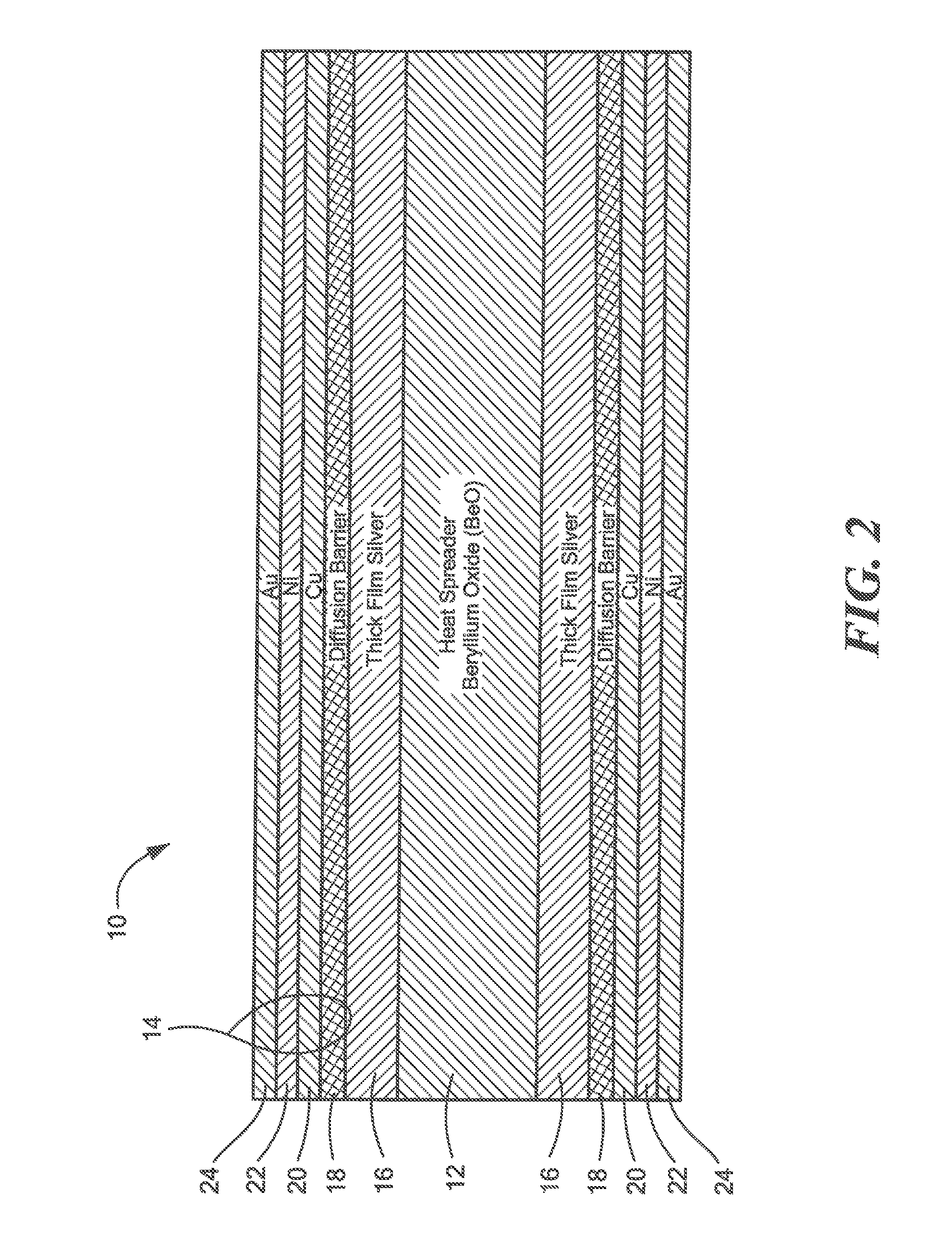
[0027]Referring now to FIG. 2 a heat spreader 10 is shown to include a ceramic substrate here for example beryllium oxide (BeO) although other materials may he used such as for example, alumina or aluminum nitride; and a metallization layer structure 14 disposed on at least one surface of the substrate 12, here on the top, horizontal, surface 13, for mounting to a heat source, such as an Monolithic Microwave Integrated Circuit chip, not shown, and the bottom horizontal surface 15, for mounting to a heat sink, not shown.

[0028]Here, the a metallization layer structure 14 includes: a thick film layer 16; a diffusion barrier layer 18 on, and in direct contact with the thick film layer 16; a heat conducting layer 20, here copper (Cu) or silver (Ag), disposed on, and in direct contact with, the diffusion barrier layer 18, a layer 22 of nickel (Ni) on the copper or silver layer 20, and a layer 24 of gold, as indicated in FIG. 2, or silver or tin, as mentioned in the example described below...


PUM


Abstract

A heat spreader provided having: as ceramic substrate; and metallization layer structure disposed on at least one surface of the substrate. The metallization layer structure includes: a thick film layer disposed on the at least one surface of the substrate; a diffusion barrier layer on, and in direct contact with the thick film layer; and as heat conducting layer disposed on, and in direct contact with, the diffusion barrier layer. The diffusion barrier layer inhibits material in the thick film layer and material in the heat conducting layer from diffusing between the thick film layer and the heat conductive layer. The metallization layer structure is disposed on a plurality of sides of the substrate.

Description

TECHNICAL FIELD[0001]This disclosure relates generally to thermal heat spreaders and more particularly to heat spreaders for high power dissipating semiconductor devices.BACKGROUND AND SUMMARY[0002]As is known in the art, heat spreaders are used to spread heat generated from a heat source, such as heat generated in an electrical circuit, and then thermally conduct the spread heat to a heat sink. As is also known in the art, in order to meet cost and performance goals, Monolithic Microwave Integrated Circuit (MMIC) devices are moving away from coplanar waveguide (CPW) designs to microstrip designs, allowing for higher wafer packing densities exacerbating the need for a high performance thermal stack. The MMIC devices having for example Gallium Nitride (GaN) epitaxial layer on a silicon carbide (SiC) substrate, for example, is processed by sometimes being thinned from 500 micron substrate to 100 or 50 micron substrate thickness depending on the process and frequency requirement. This ...

Claims


Application Information

Patent Timeline
IPC IPC(8): H01L23/34F28F21/08
CPCH01L23/34F28F21/089F28F21/087F28F21/085H01L23/373H01L23/3731H01L23/3735
Inventor TRULLI, SUSAN C.
Owner RAYTHEON CO
Why Eureka
Try Eureka