

Solar cell, manufacturing method therefor, semiconductor device, and manufacturing method therefor
- Summary
- Abstract
- Description
- Claims
- Application Information
AI Technical Summary
Benefits of technology
Problems solved by technology
Method used
Image

Examples
first embodiment
[0048]A solar cell according to a first embodiment of the present invention includes at least a first semiconductor layer and a second semiconductor layer. The first semiconductor layer is a layer including metal oxide particles of 1 nm or more and 500 nm or less (hereinafter 1 to 500 nm) in average particle size, and a compound having relative permittivity of 2 or more.
[0049]Firstly, the following describes materials and physical properties of the metal oxide particles, the compound having relative permittivity of 2 or more, the semiconductor layer and the junction interface layer. Next the structure of the solar cell is described.
[0050]Examples of oxides used for metal oxide particles include metal oxides, such as copper oxide (I), copper oxide (II), iron oxide, zinc oxide, silver oxide, titanium oxide (rutile, anatase), zinc oxide doped with aluminum (AZO), zinc oxide doped with gallium (GZO), indium tin oxide (ITO), tin oxide, tin oxide doped with fluorine...
first example
(1) First Example
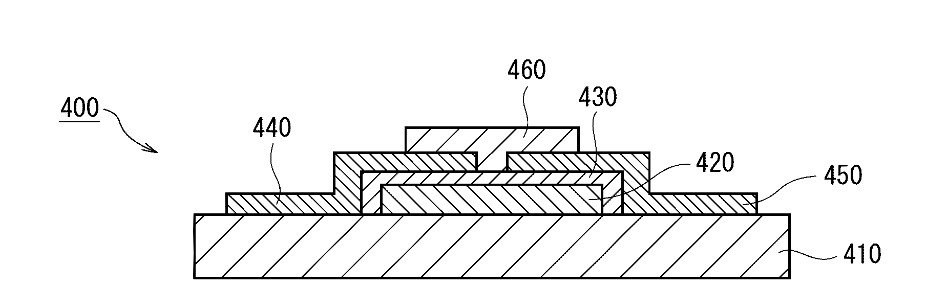
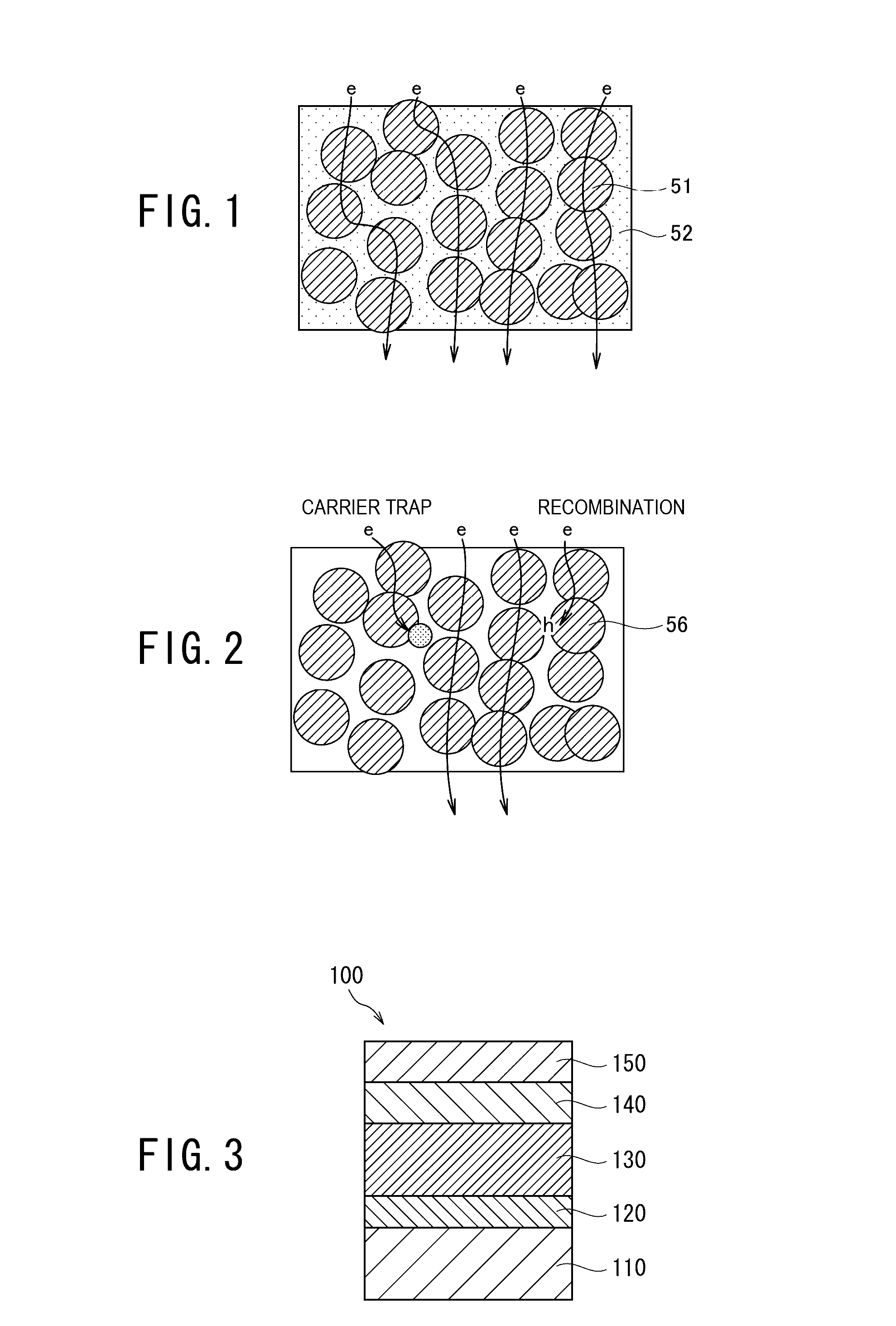
[0164]FIG. 3 is a cross-sectional view schematically illustrating an exemplary structure of a solar cell 100 according to the first embodiment.
[0165]As illustrated in FIG. 3, this solar cell 100 includes a substrate 110, an anode layer 120 formed on the substrate 110, a second semiconductor layer 130 formed on the anode layer 120, a first semiconductor layer 140 formed on the second semiconductor layer 130, and a cathode layer 150 formed on the first semiconductor layer 140. The first semiconductor layer 140 is the “semiconductor layer including metal oxide particles and compound having relative permittivity of 2 or more” as stated above. The second semiconductor layer 130 is the “semiconductor layer made of semiconductor” as stated above.
[0166]When the solar cell 100 in FIG. 3 is of a p-p junction type, both of the first semiconductor layer 140 and the second semiconductor layer 130 are a p-type semiconductor layer, where the second semiconductor layer 130 has high...
second example
(2) Second Example
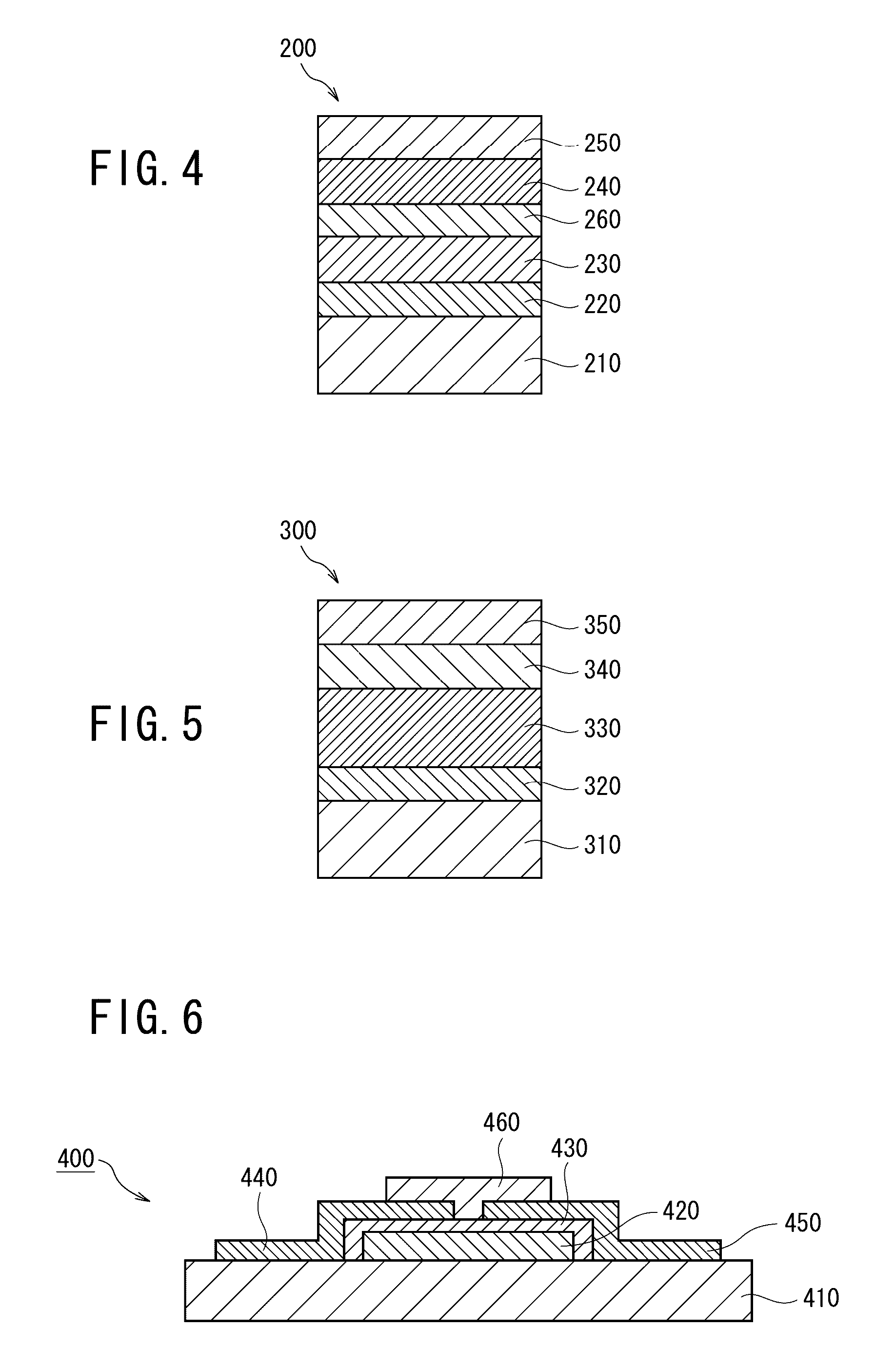
[0169]FIG. 4 is a cross-sectional view schematically illustrating an exemplary structure of a solar cell 200 according to the first embodiment of the present invention.
[0170]The solar cell 200 illustrated in FIG. 4 includes a substrate 210, an anode layer 220 formed on the substrate 210, a second semiconductor layer 230 formed on the anode layer 220, a junction interface layer 260 formed on the second semiconductor layer 230, a first semiconductor layer 240 formed on the junction interface layer 260, and a cathode layer 250 formed on the first semiconductor layer 240. The junction interface layer 260 includes a compound having relative permittivity of 2 or more. The first semiconductor layer 240 is the “semiconductor layer including metal oxide particles and compound having relative permittivity of 2 or more” as stated above. The second semiconductor layer 230 is the “semiconductor layer made of semiconductor” as stated above.
[0171]When the solar cell 200 in FIG. 4...
PUM
 Abstract
Description
Claims
Application Information