Seal ring structure to avoid delamination defect

a ring structure and delamination defect technology, applied in the field of semiconductor devices, can solve the problems of delamination defects, cracking, peeling, and finished products after laser grooving and diamond cutting processes, and conventional methods cannot prevent delamination from occurring, so as to improve the yield and performance of the semiconductor devi

Active Publication Date: 2016-11-24
SEMICON MFG INT (SHANGHAI) CORP
View PDF1 Cites 4 Cited by
  • Summary
  • Abstract
  • Description
  • Claims
  • Application Information

AI Technical Summary

Benefits of technology

[0023]In accordance with the present invention, the seal ring structure can effectively buffer the stress generated by cutting the semiconductor substrate to protect the integrate

Problems solved by technology

However, with the continuous shrinking of the size of the semiconductor devices, in processing semiconductor devices with technology nodes of 40 nm and below, the finished products after the laser grooving and diamond cutting processes suffer cracking, peeling, and delamination defects.
However, the conventional methods cannot prevent delamination from occurring.
Conventional seal rings cannot stop delamination, low dielectric const

Method used


Image

  • Seal ring structure to avoid delamination defect
  • Seal ring structure to avoid delamination defect
  • Seal ring structure to avoid delamination defect

Examples


first embodiment

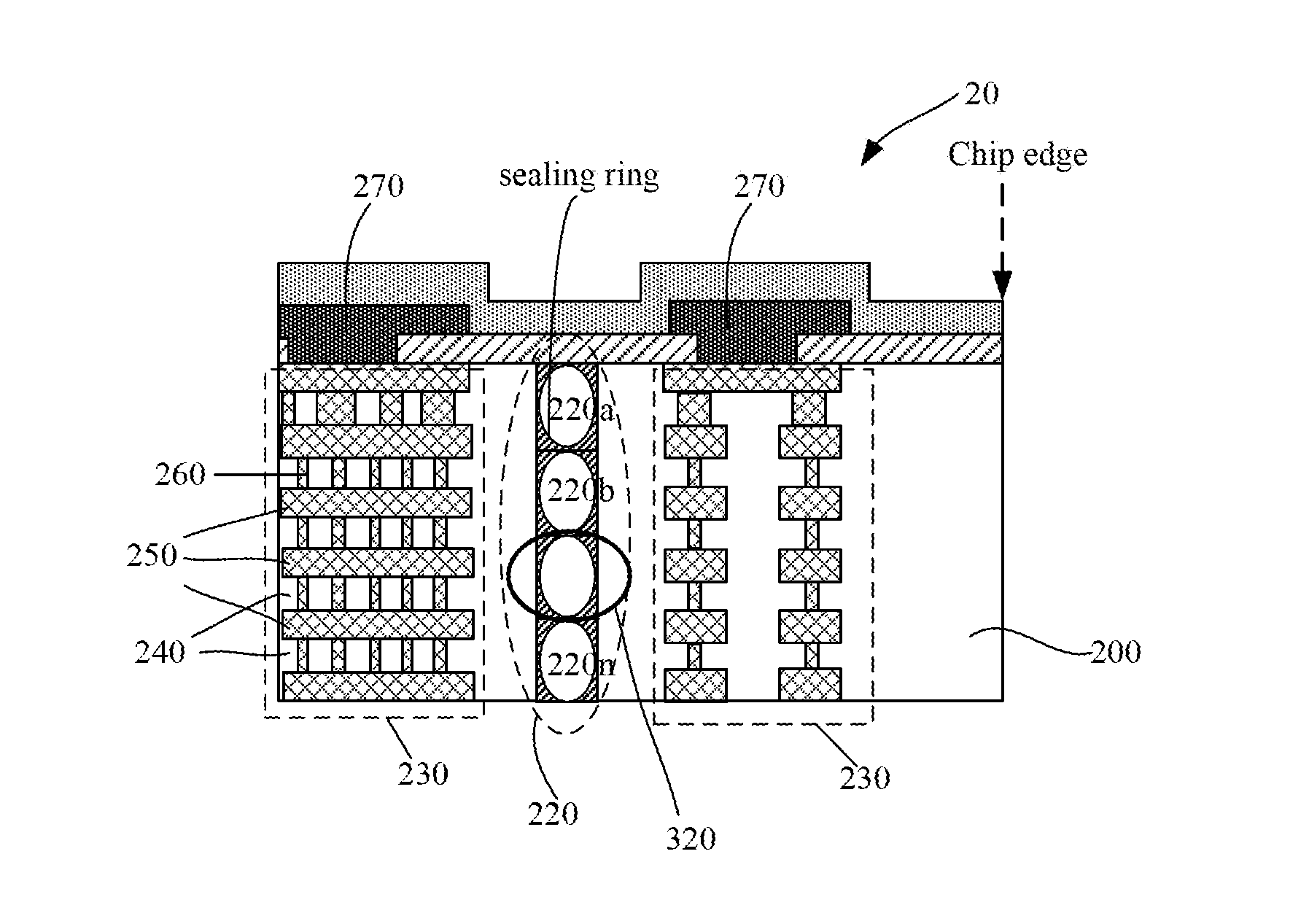
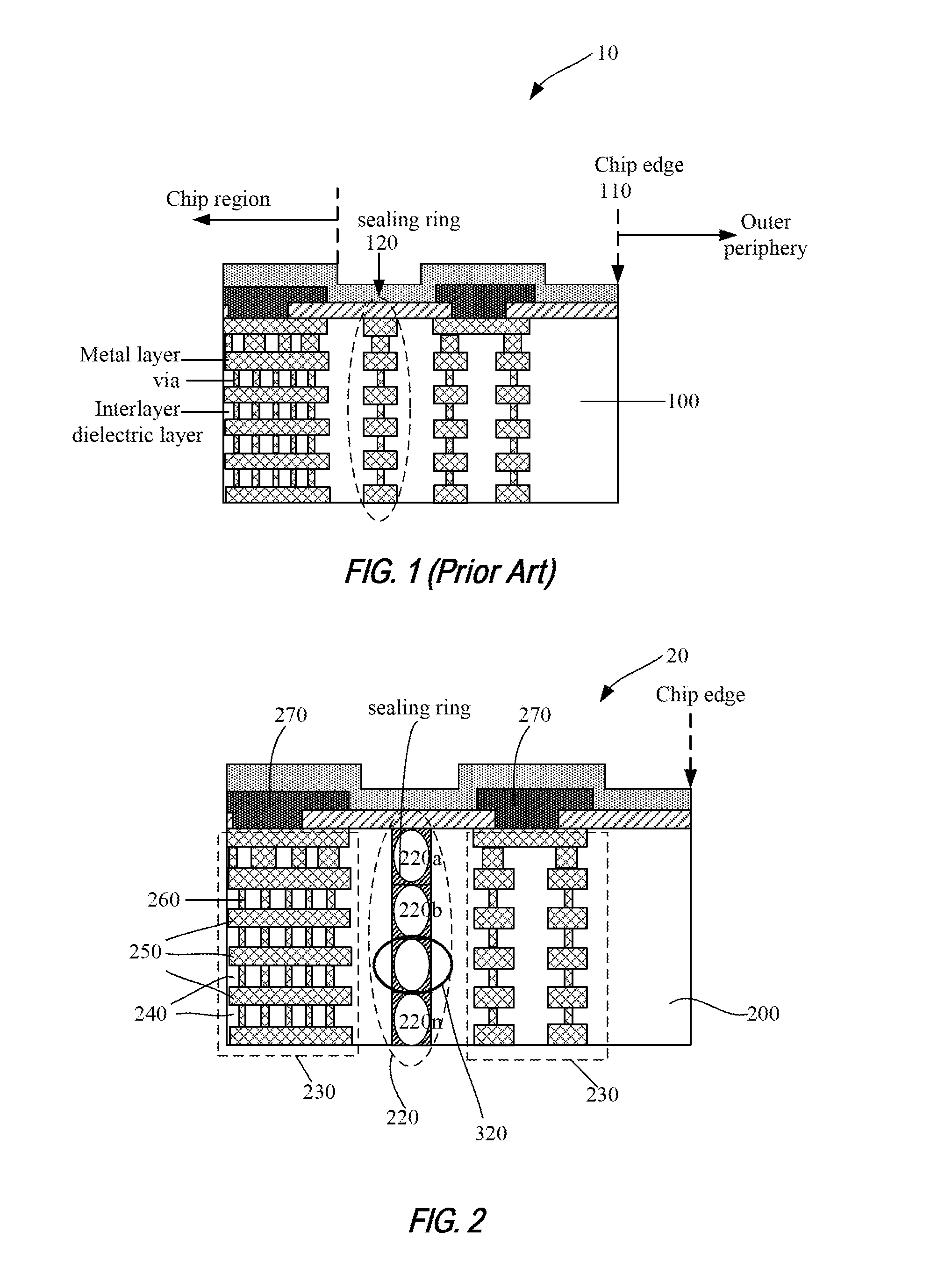
[0037]FIG. 2 is a cross-sectional view of a semiconductor device including a seal ring structure according to one embodiment of the present invention. Referring to FIG. 2, a semiconductor device (alternatively referred to as chip or integrated circuit device) 20 includes a semiconductor substrate 200. The semiconductor substrate may be made of silicon, silicon-on-insulator (SOI), strained silicon-on-insulator (SSOI), strained silicon germanium on insulator (S—SiGeOI), silicon germanium on insulator (SiGeOI), germanium on insulator (GeOI) and the like.

[0038]The semiconductor device 20 may also include multiple chips (not shown) on the semiconductor substrate. Each chip may include a complete integrated circuit structure, the integrated circuit is provided in the active region of the semiconductor substrate. In the semiconductor manufacturing processes, a dicing process is performed to cut the semiconductor substrate into multiple fully functional integrated circuit devices. The dicin...

second embodiment

[0048]Embodiments of the present invention also provide a method for manufacturing a semiconductor device. The method may include:

[0049]at A1: providing a semiconductor substrate, and forming one or more integrated circuit devices (semiconductor devices, ICs, or chips) on the semiconductor substrate. The semiconductor substrate may be made of silicon, silicon-on-insulator (SOI), strained silicon-on-insulator (SSOI), strained silicon germanium on insulator (S—SiGeOI), silicon germanium on insulator (SiGeOI), germanium on insulator (GeOI) and the like.

[0050]Each of the integrated circuit devices includes a complete integrated circuit structure (including transistors, capacitors, resistors, diodes, etc.) disposed in an active region of the semiconductor substrate.

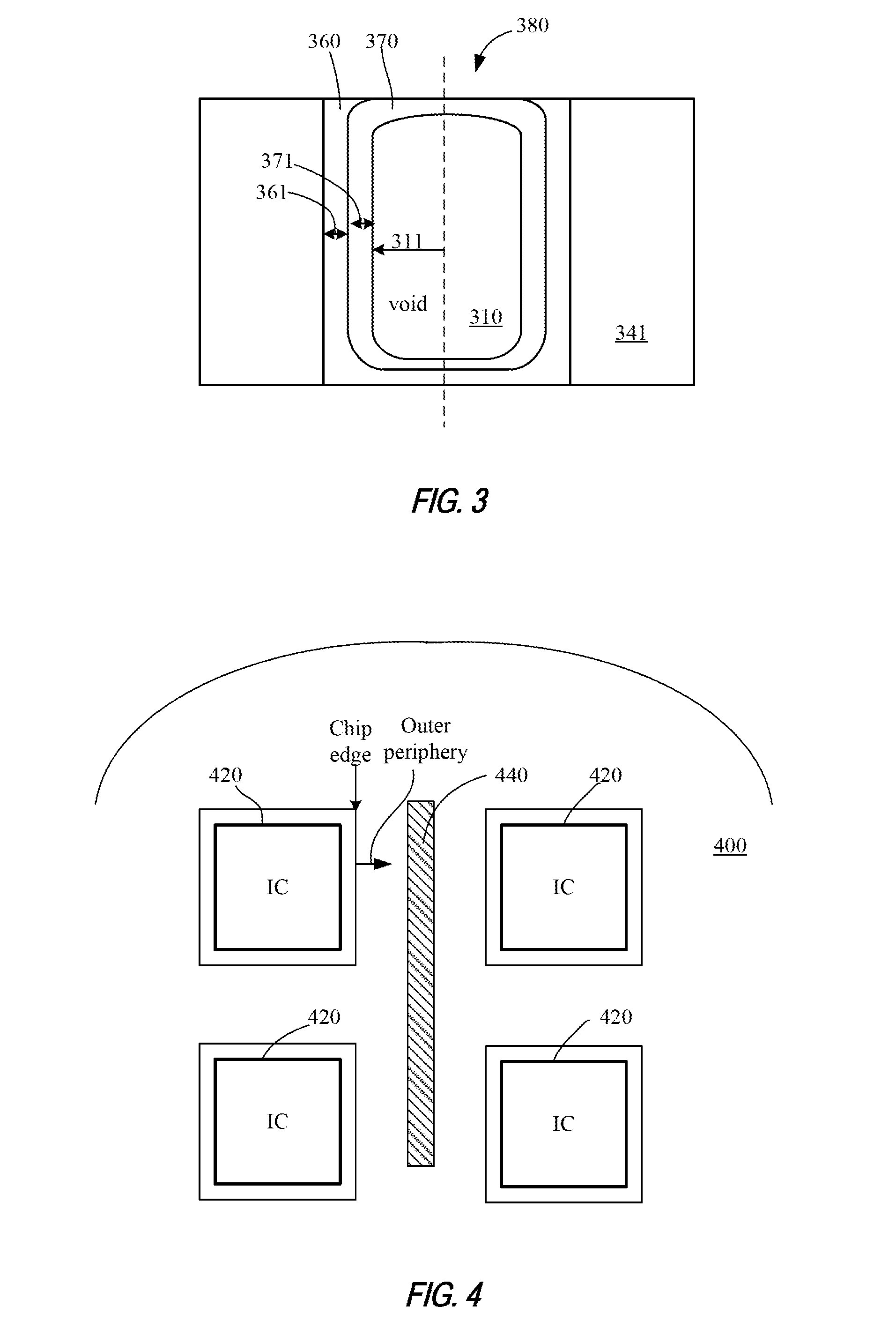
[0051]at A2: forming a seal ring structure (alternatively referred to as seal ring) surrounding each of the integrated circuit devices (chips). The seal ring structure includes multiple interlayer dielectric layers and hollow ...

third embodiment

[0060]Embodiments of the present invention provide an electronic device including an electronic component and a semiconductor device connected to the electronic component. The semiconductor device can be the semiconductor device of embodiment 1 or manufactured by the above-described method of embodiment 2.

[0061]In accordance with the present invention, the electronic device may be a mobile phone, a laptop computer, a netbook, a tablet PC, a game console, a TV, a DVD player, a GPS device, a camera, a voice recorder, MP3, MP4, PSP players, and other semiconductor devices including intermediate products and electronic components that are manufactured using the above-described method to improve RF performance.


PUM


Abstract

A semiconductor device includes a semiconductor substrate, a plurality of integrated circuit devices on the semiconductor substrate, and a seal ring structure surrounding each one of the integrated circuit devices. The seal ring structure includes a plurality of interlayer dielectric layers and a plurality of hollow through-hole structures disposed within each of the interlayer dielectric layers. Each of the hollow through-hole structure within an interlayer dielectric layer includes a through-hole disposed within one of the interlayer dielectric layers, a diffusion barrier layer formed at the bottom, sidewalls and the top of the through-hole, and a seed layer disposed on the diffusion barrier layer. The diffusion barrier layer and the seed layer cover the top of the through-hole so that the through-hole has a void to form the hollow through-hole structure.

Description

CROSS-REFERENCES TO RELATED APPLICATIONS[0001]This application claims priority to Chinese patent application No. 201510255840.7, filed May 19, 2015, the content of which is incorporated herein by reference in its entirety.FIELD OF INVENTION[0002]The present invention relates to semiconductor technology, and more particularly to a semiconductor device and manufacturing method thereof.BACKGROUND OF THE INVENTION[0003]In the manufacture of microelectronic devices, integrated circuits are formed on a semiconductor substrate, which generally includes silicon or other materials such as gallium arsenide, and a plurality of interconnect layers such as copper layers, aluminum layers, and the like. With the development of semiconductor technology and integrated circuits, semiconductor technology continues to advance to smaller technology nodes, a semiconductor substrate may include an increased number of integrated circuits. The processed semiconductor substrate is then cut into a number of f...

Claims


Application Information

Patent Timeline
IPC IPC(8): H01L23/00H01L23/532H01L21/768H01L21/78
CPCH01L23/562H01L21/76847H01L23/53238H01L21/78
Inventor LING, LONG
Owner SEMICON MFG INT (SHANGHAI) CORP
Why Eureka
Try Eureka