Photosensitization chemical-amplification type resist material, method for forming pattern using same, semiconductor device, mask for lithography, and template for nanoimprinting

a chemical amplification and resist material technology, applied in the direction of photomechanical equipment, originals for photomechanical treatment, instruments, etc., can solve the problems of difficult to achieve both higher sensitivity and better lithography characteristics, and achieve the effect of high sensitivity and extremely excellent lithography characteristics

Active Publication Date: 2016-12-08
TOKYO ELECTRON LTD +1
View PDF5 Cites 35 Cited by
  • Summary
  • Abstract
  • Description
  • Claims
  • Application Information

AI Technical Summary

Benefits of technology

[0012]According to the present invention, there is provided a chemical-amplification type resist material which makes it possible to achieve both of high sensitivity and extremely excellent lithography characteristics in a pattern forming technique using ionizing radiation such as EUV light, electron beams or ion beams, or non-ionizing radiation having a wavelength of equal to or less than 400 nm such as a KrF excimer laser or an ArF excimer laser. Furthermore, according to the present invention, there are provided a method for forming a pattern, a semiconductor device, a mask for lithography, and a template for nanoimprinting using the resist material.

Problems solved by technology

With the technique of the related art, it is difficult to achieve both of higher sensitivity and better lithography characteristics (high resolution, low pattern roughness, and the like).

Method used


Image

  • Photosensitization chemical-amplification type resist material, method for forming pattern using same, semiconductor device, mask for lithography, and template for nanoimprinting
  • Photosensitization chemical-amplification type resist material, method for forming pattern using same, semiconductor device, mask for lithography, and template for nanoimprinting
  • Photosensitization chemical-amplification type resist material, method for forming pattern using same, semiconductor device, mask for lithography, and template for nanoimprinting

Examples


first embodiment

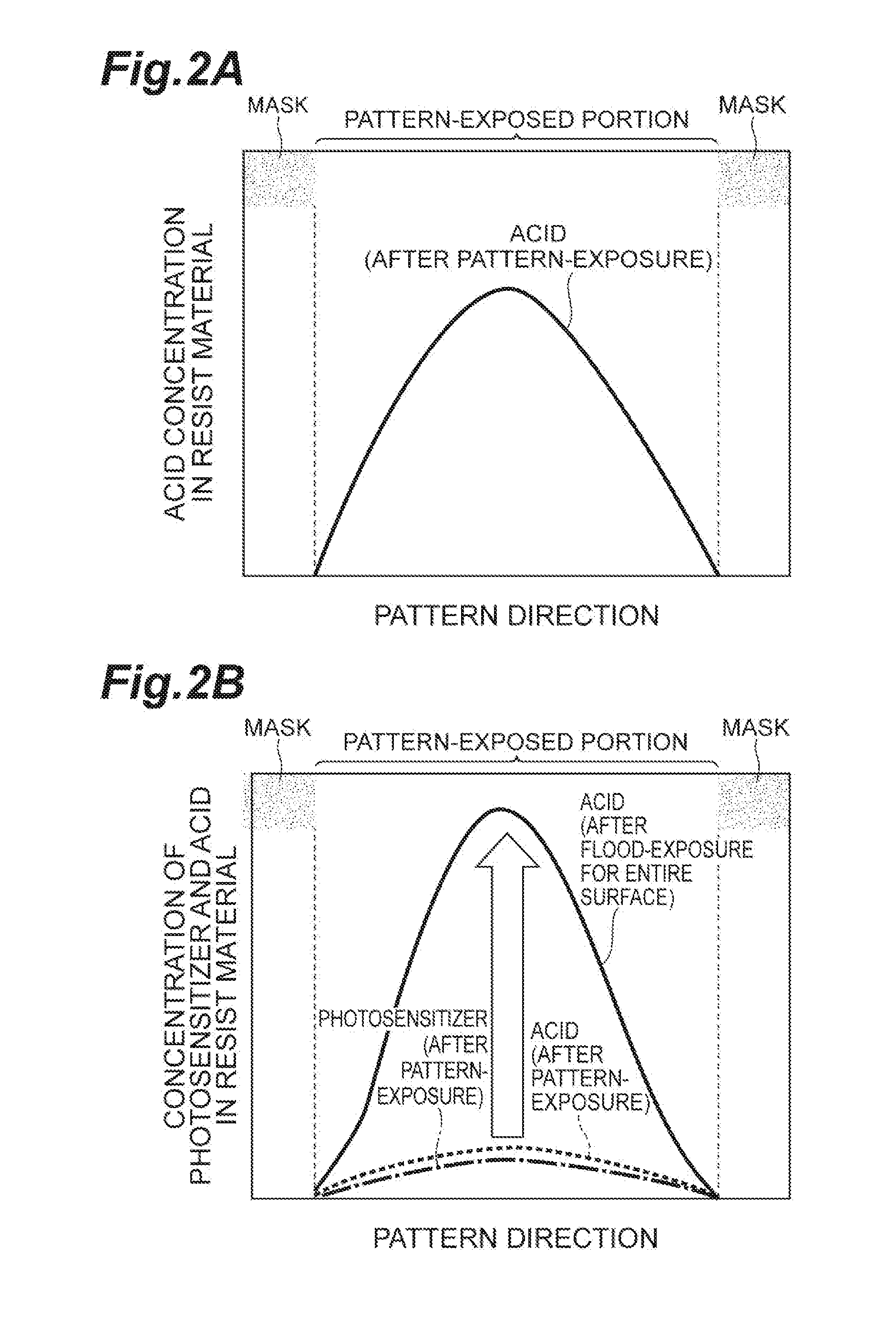
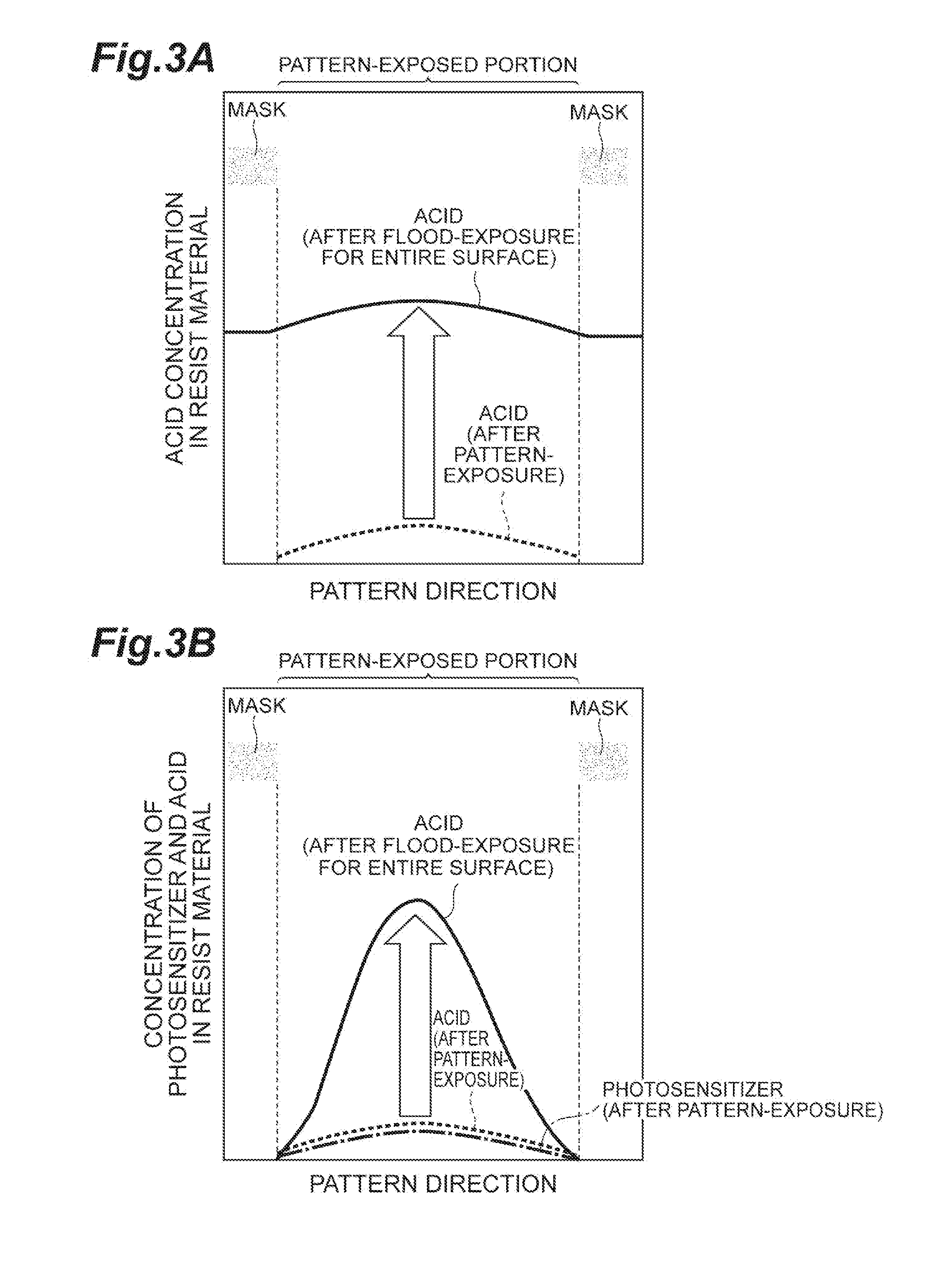
[0033]The photosensitization chemical-amplification type resist material according to the present embodiment (hereinafter, simply referred to as a “resist material” in some cases) contains (1) a base component and (2) a component generating a photosensitizer and an acid by exposure.

[0034](1) Base Component

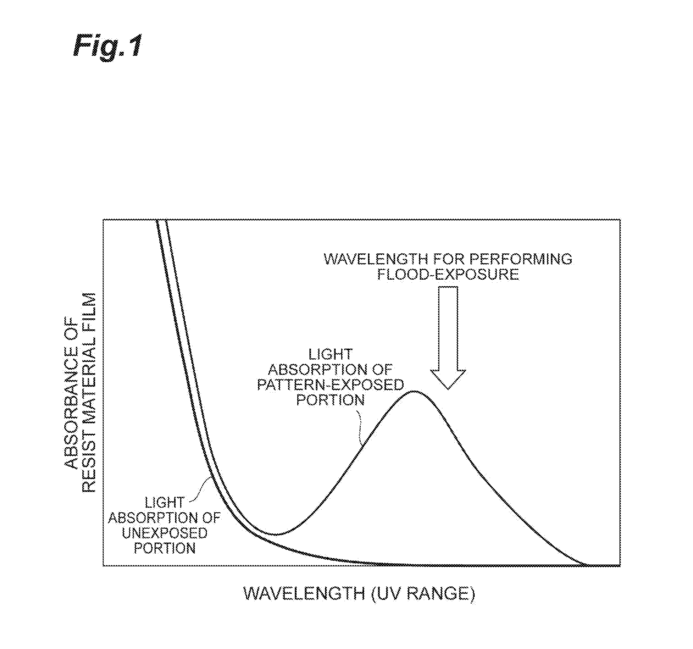
[0035]In the present embodiment, the (1) base component may be an organic compound or an inorganic compound. The organic compound may be a polymer compound or a low-molecular weight compound. It is desired that the base component does not excessively absorb the first radiation in the pattern-exposure and enables the formation of a resist pattern with a shape having sufficiently high verticality. Furthermore, it is desired that the base component absorbs little the second radiation in the flood-exposure and hardly causes an unnecessary sensitization reaction in an unexposed portion at the time of flood-exposure.

[0036]The polymer compound is a compound which has a weight average mole...

second embodiment

[0150]A photosensitization chemical-amplification type resist material (hereinafter, simply referred to as a “resist material” in some cases) of the present embodiment contains (1′) a base component which makes a pattern-exposed portion soluble or insoluble in a developer after the baking step.

[0151](1′) Base Component

[0152]The (1′) base component may be an organic compound or an inorganic compound. Furthermore, the organic compound may be a polymer compound or a low-molecular weight compound. The (1′) base component has, among three groups consisting of (d) an acid-photosensitizer generating group, (e) a precursor group, and (f) a photoacid generating group, only the group (d), any two groups, or all of the groups (d) to (f) described below. That is, in the present embodiment, the base component is an organic or inorganic compound to which the following groups (d) to (f) are bonded. The base component may have the following groups (d) to (f) in a single molecule (or a single partic...

example 1

[0308]32.19 parts by mass (0.44 parts by mole) of the following GBLMA, 23.86 parts by mass (0.24 parts by mole) of the following MAMA, and 21.29 parts by mass (0.21 parts by mole) of the following HAMA as methyl methacrylates to which a protecting group was bonded and 22.66 parts by mass (0.11 parts by mole) of the following PBpS-F2MAS as methyl methacrylate to which a photoacid generating group was bonded were mixed together and radically polymerized, thereby synthesizing a methyl methacrylate-based polymer compound (polymer compound P) having the (f) photoacid generating group as the component (1′). The obtained methyl methacrylate-based polymer compound had a weight average molecular weight (Mw) of 24,800 and a molecular weight distribution (Mw / Mn) of 3.08. Herein, the above Mw and Mw / Mn were measured through gel permeation chromatography (GPC) under the following conditions by using a calibration curve based on standard polystyrene.

Device: HPLC (manufactured by Shimadzu Corporat...


PUM

PropertyMeasurementUnit
wavelengthaaaaaaaaaa
refractive indexaaaaaaaaaa

Abstract

A photosensitization chemical-amplification type resist material according to the present invention is used for a two-stage exposure lithography process, and contains (1) a developable base component and (2) a component generating a photosensitizer and an acid through exposure. Among three components consisting of (a) an acid-photosensitizer generator, (b) a photosensitizer precursor, and (c) a photoacid generator, the above component contains only the component (a), any two components, or all of the components (a) to (c).

Description

TECHNICAL FIELD[0001]The present invention relates to a photosensitization chemical-amplification type resist material, a method for forming a pattern using the same, a semiconductor device, a mask for lithography, and a template for nanoimprinting.BACKGROUND ART[0002]As one of the fundamental techniques for manufacturing next-generation semiconductor devices, extreme ultraviolet ray (EUV) lithography is drawing attention. EUV lithography is a pattern forming technique using BUY light having a wavelength of 13.5 nm as an exposure light source. EUV lithography has been demonstrated to be able to form an extremely fine pattern (for example, equal to or smaller than 20 nm) in an exposure step of a semiconductor device manufacturing process.[0003]However, because EUV light sources having been developed at this point in time have low power, the exposure treatment takes a long time, and hence EUV lithography has currently not yet been put to practical use. In order to compensate for the l...

Claims


Application Information

Patent Timeline
Patent Type & Authority Applications(United States)
IPC IPC(8): G03F7/039G03F7/16G03F7/20G03F1/26G03F7/32G03F1/20G03F1/24G03F7/004G03F7/38
CPCG03F7/0397G03F7/0045G03F7/16G03F7/2002G03F1/26G03F7/322G03F7/2041G03F1/20G03F1/24G03F7/38G03F7/0382G03F7/2022C08F220/283C08F220/382G03F7/0002G03F7/32G03F7/70308G03F7/70575C07C381/12C07C309/07C07C303/32H01L21/0274C08F220/14C08F220/22
Inventor NAGAHARA, SEIJITAGAWA, SEIICHIOSHIMA, AKIHIRO
Owner TOKYO ELECTRON LTD
Why Eureka
Try Eureka