Tuned semiconductor amplifier

a technology of semiconductor transistors and amplifiers, applied in the direction of multiple-port active networks, cad circuit design, impedence matching networks, etc., can solve the problems of placing austere performance demands on rf power transistors, and achieve the effect of improving the performance of high-speed, high-power, semiconductor transistors

Active Publication Date: 2017-04-13
MACOM TECH SOLUTIONS HLDG INC
View PDF0 Cites 9 Cited by
  • Summary
  • Abstract
  • Description
  • Claims
  • Application Information

AI Technical Summary

Benefits of technology

[0007]Methods and structures for improving the performance of high-speed, high-power, semiconductor transistors are described. The transistors may comprise gallium-nitride material in some embodiments, though other semiconductor materials may be used on other embodiments. In some implementations, the transistors may be formed from one or more layers of gallium nitride semiconductor material deposited on a substrate of a different material. On-chip circuitry may be included to tune the performance of the device to suppress second harmonic generation and match an input impedance of the device. According to some embodiments, a two-capacitor input network is incorporated into a transistor package to improve the performance of the device.

Problems solved by technology

Applications supporting mobile communications and wireless internet access under current and proposed communication standards, such as WiMax, 4G, and 5G, can place austere performance demands on RF power transistors.

Method used


Image

  • Tuned semiconductor amplifier
  • Tuned semiconductor amplifier
  • Tuned semiconductor amplifier

Examples


example

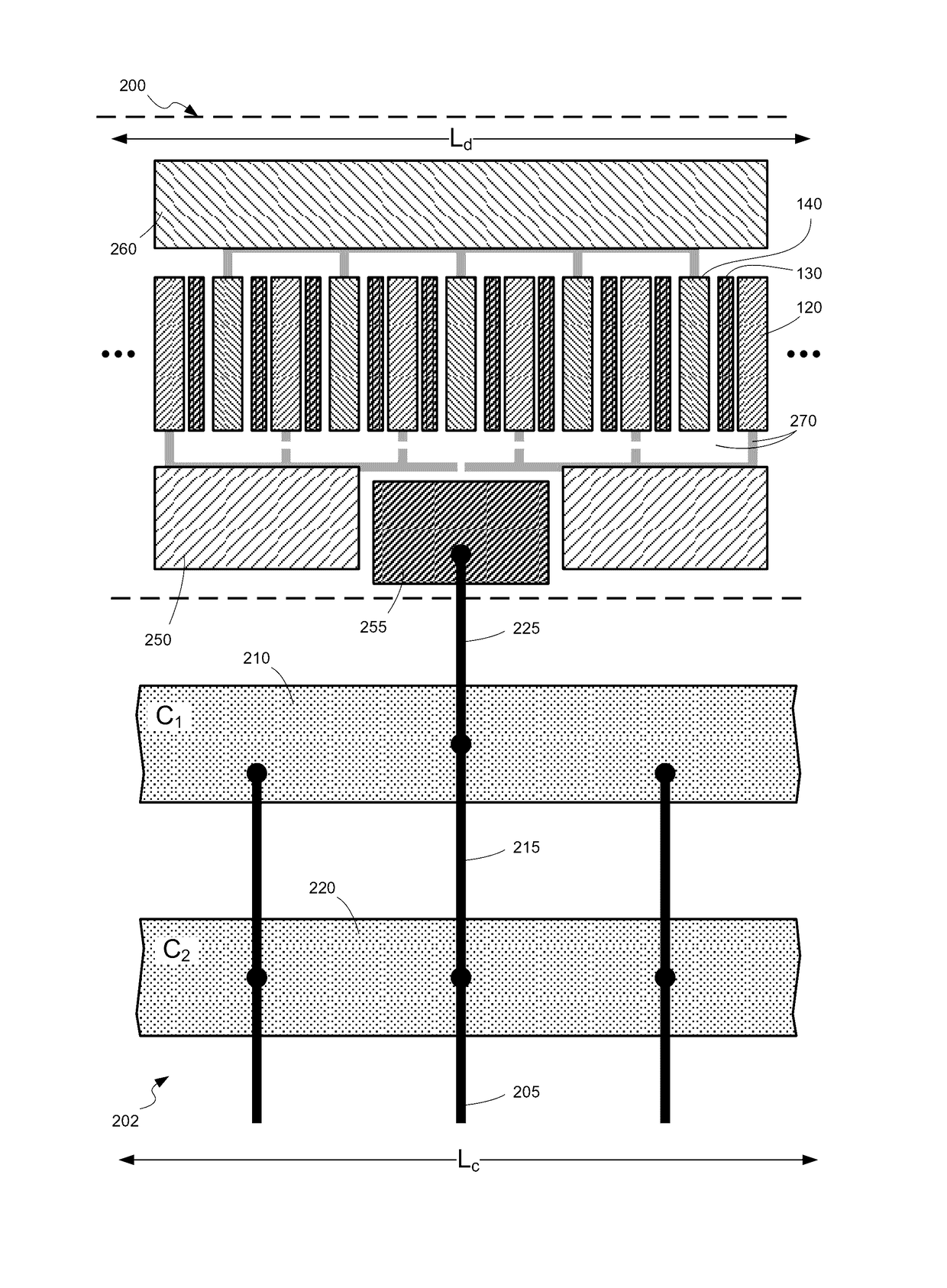
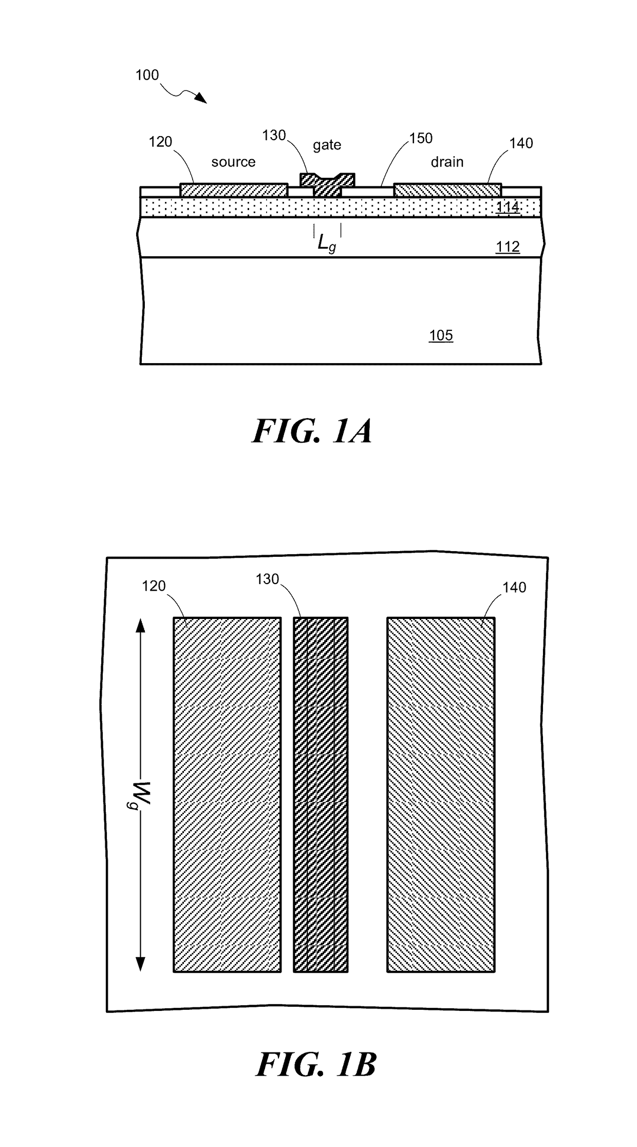
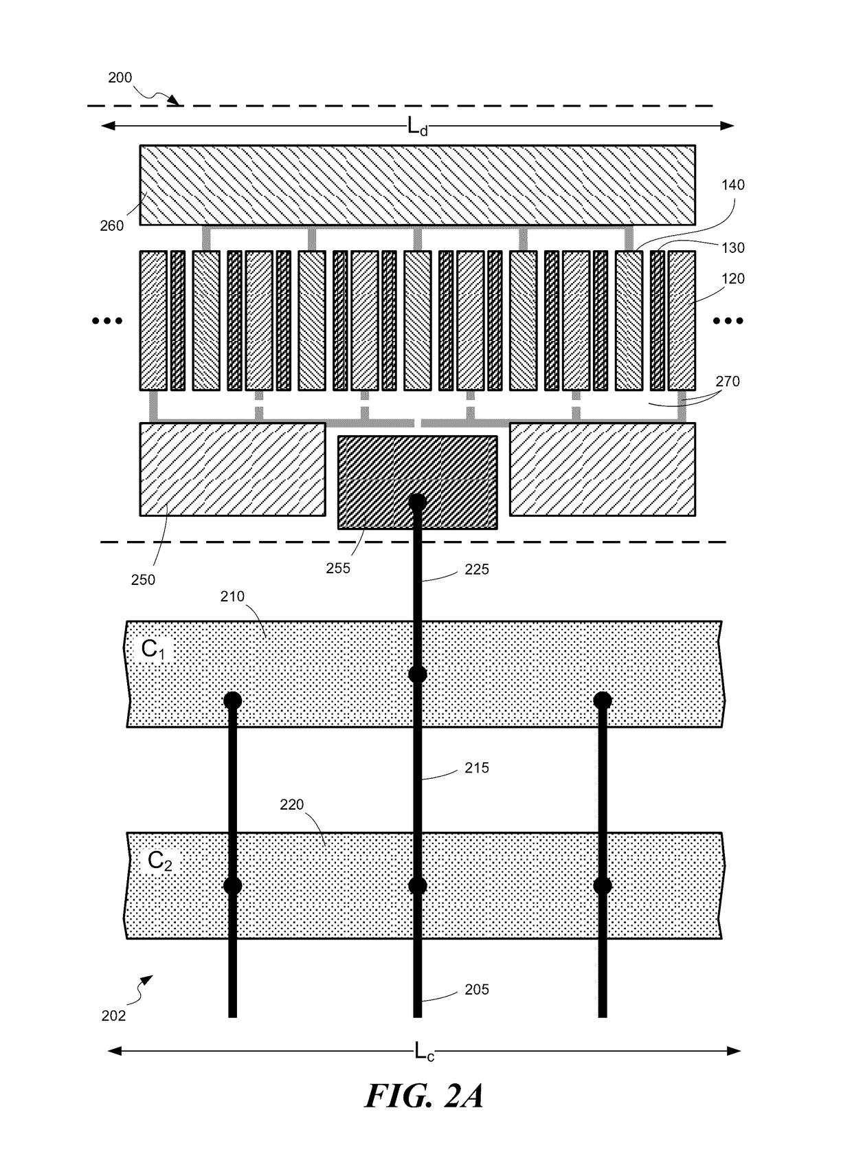
[0071]This example illustrates a tuning process for one embodiment of a gallium-nitride power transistor. The transistor package was similar to that depicted in FIG. 2B, and the periphery value for the active region of the transistor was approximately 24.2 mm. Twelve bond wires were connected between gate pads 255 of the transistor and a first capacitor C1 of a first capacitive shunt. The first capacitive shunt was located off die, but within the transistor package. The bond wires were spaced on a pitch of approximately 380 microns. The bond wires were gold having a diameter of approximately 25 microns. In the first stage of tuning, the capacitor C1 was adjusted to locate the resonance loop peak 320 of the S11 curve at approximately 5300 MHz, as depicted in FIG. 6A. The gate-to-source capacitance Cgs was included in the model. The value of capacitor C1 was selected to be 20 pF.

[0072]For reference, the source-terminal impedance curve (which provides a measure of impedance looking fro...


PUM


Abstract

Methods and structures for improving the performance of integrated semiconductor transistors operating at high frequency and / or high power are described. Two capacitors may be connected to an input of a semiconductor transistor and tuned to suppress second-harmonic generation and to transform and match the input impedance of the device. A two-stage tuning procedure is described. The transistor may comprise gallium nitride and may be configured as a power transistor capable of handling up to 1000 W of power. A tuned transistor may operate at frequencies up to 6 GHz with a peak drain efficiency greater than 60%.

Description

BACKGROUND[0001]Technical Field[0002]The technology relates to high-speed, high-power semiconductor transistors and amplifiers constructed from such transistors.[0003]Discussion of the Related Art[0004]Gallium nitride semiconductor material has received appreciable attention in recent years because of its desirable electronic and electro-optical properties. GaN has a wide, direct bandgap of about 3.4 eV that corresponds to the blue wavelength region of the visible spectrum. Light-emitting diodes (LEDs) and laser diodes (LDs) based on GaN and its alloys have been developed and are commercially available. These devices can emit visible light ranging from the violet to red regions of the visible spectrum.[0005]Because of its wide bandgap, GaN is more resistant to avalanche breakdown and can maintain electrical performance at higher temperatures than other semiconductors, such as silicon. GaN also has a higher carrier saturation velocity compared to silicon. Additionally, GaN has a Wurt...

Claims


Application Information

Patent Timeline
Patent Type & Authority Applications(United States)
IPC IPC(8): H01L29/20H01L27/088H01L23/532H01L29/778H01L29/267H01L23/528H03H11/28H01L49/02
CPCH01L29/2003H03H11/28H01L27/088H01L23/53242H01L29/778H01L29/267H01L23/528H01L28/60H01L21/50H01L25/16H03F1/56H03F3/191H03F3/21H03F2200/451H01L23/642H03F3/193H03F3/20H03F2200/222H03F2200/75H01L2224/49175H01L29/41758H01L29/7783H01L2924/00014H01L2224/45015H01L2224/45144H01L2224/4813H01L2924/381H01L2924/13091H01L2224/04042H01L2224/48195H01L2924/19107H01L2924/19105H01L2924/19041H01L2924/3011H01L2224/49111H01L2224/45014H01L2224/48247H01L2223/6611H01L24/45H01L24/48H01L24/49H01L23/66H01L2223/6655G06F30/36H01L2924/20752H01L2924/00H03F3/211H03H7/38H01L23/64H01L2224/45644
Inventor NAGY, WALTER H.PATTISON, LYNDON
Owner MACOM TECH SOLUTIONS HLDG INC
Why Eureka
Try Eureka