Metal halide perovskite light emitting device and method of manufacturing the same

a technology of light-emitting devices and metal halide perovskite, which is applied in the direction of solid-state devices, chemistry apparatuses and processes, and light-emitting compositions. it can solve the problems of color purity deterioration, difficult adjustment of the size of the quantum dot during the synthesis process, and inability to manufacture low-priced products. it can reduce the grain size and improve the electrical characteristics. , the effect of improving the quality

Inactive Publication Date: 2017-05-04
POSTECH ACAD IND FOUND
View PDF1 Cites 19 Cited by
  • Summary
  • Abstract
  • Description
  • Claims
  • Application Information

AI Technical Summary

Benefits of technology

[0020]Embodiments of the present invention provide a metal halide perovskite light emitting diode and a method of manufacturing the same in which metal halide perovskites have a decreased grain size, and that has the effect of defect passivation on the metal halide perovskites and improved electrical characteristics, through a two-step process in which an organic solution in which a low-molecular-weight organic substance is dissolved in a small amount in an organic solvent is additionally applied before a solvent is removed from a light emitting layer during formation of a metal halide perovskite light emitting layer.

Problems solved by technology

However, although organic light emitting diodes have high efficiency, they have a drawback in that color purity may deteriorate due to a wide full width at half maximum of an emission spectrum, and while inorganic quantum dots in which color is adjusted according to the size of the quantum dots have high color purity, they have a drawback in that it is very difficult to adjust the size of the quantum dot during a synthesis process.
Also, organic light emitting diodes and inorganic quantum dot materials have a limitation in manufacturing low-priced products due to their high manufacturing costs.
As a result, since the light emission in the organic ammonium does not have high color purity (a full width at half maximum of less than 30 nm), the full width at half maximum of a light emission spectrum should be wider than 50 nm, which makes the organic metal halide perovskite unsuitable for light emitting layers.
Therefore, in this case, the organic metal halide perovskite is very unsuitable for phosphors having high color purity (a full width at half maximum of less than 30 nm) emphasized in this patent application.
Although such a metal halide perovskite has advantages as a light emitting diode, the metal halide perovskite has a problem of limitations in application to light emitting diodes.
First, a problem such as a decline in efficiency of a light emitting diode is caused due to various types of defects present inside perovskites.
That is, since such defects exist out of an energy level of a conduction band or a valence band, the electrons or holes are trapped at an energy level of the defects to limit movement of charges and induce unwanted non-radiative recombination.
In light emitting diodes in which the balance between the electrons and the holes is important, perovskites having only p-type characteristics have a problem in that they can only exhibit low efficiency.
In this way, a metal halide perovskite thin film has a drawback in that it is difficult to implement using a thin film manufacturing process (in which a device having higher efficiency has a higher grain size (>200 nm) and severe surface unevenness) used in metal halide solar cells known in the art.

Method used


Image

  • Metal halide perovskite light emitting device and method of manufacturing the same
  • Metal halide perovskite light emitting device and method of manufacturing the same
  • Metal halide perovskite light emitting device and method of manufacturing the same

Examples


example 1

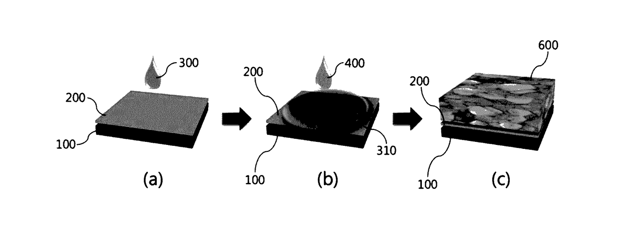
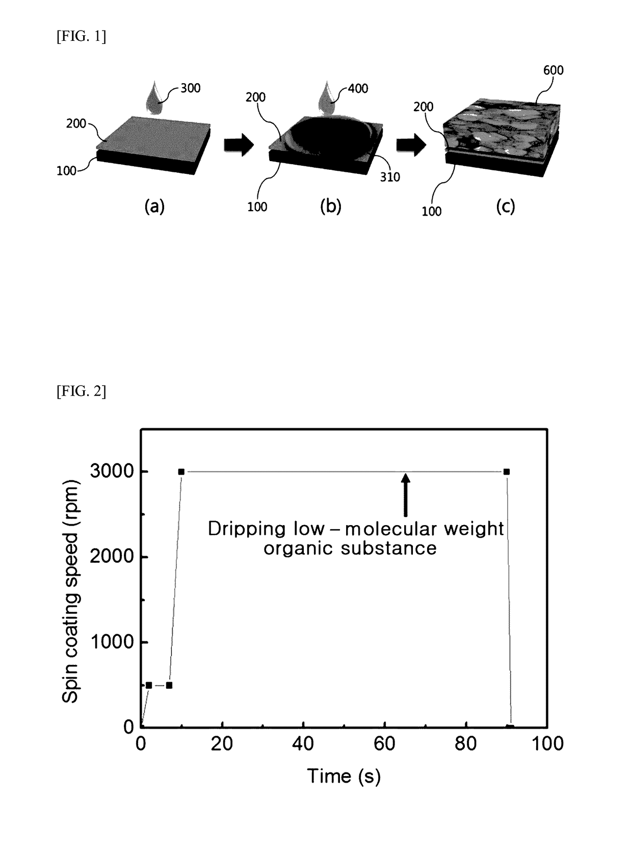
[0088]Formation of a Metal Halide Perovskite Light Emitting Layer Through Coating by Dripping a Low-Molecular-Weight Organic Substance Solution (an Organic-Substance-Assisted Nanocrystal Fixing Process)

[0089]First, CH3NH3Br and PbBr2 were mixed at a ratio of 1.05:1 and the resulting mixture was dissolved in dimethyl sulfoxide (DMSO) at 40% by weight to prepare a CH3NH3PbBr3 solution.

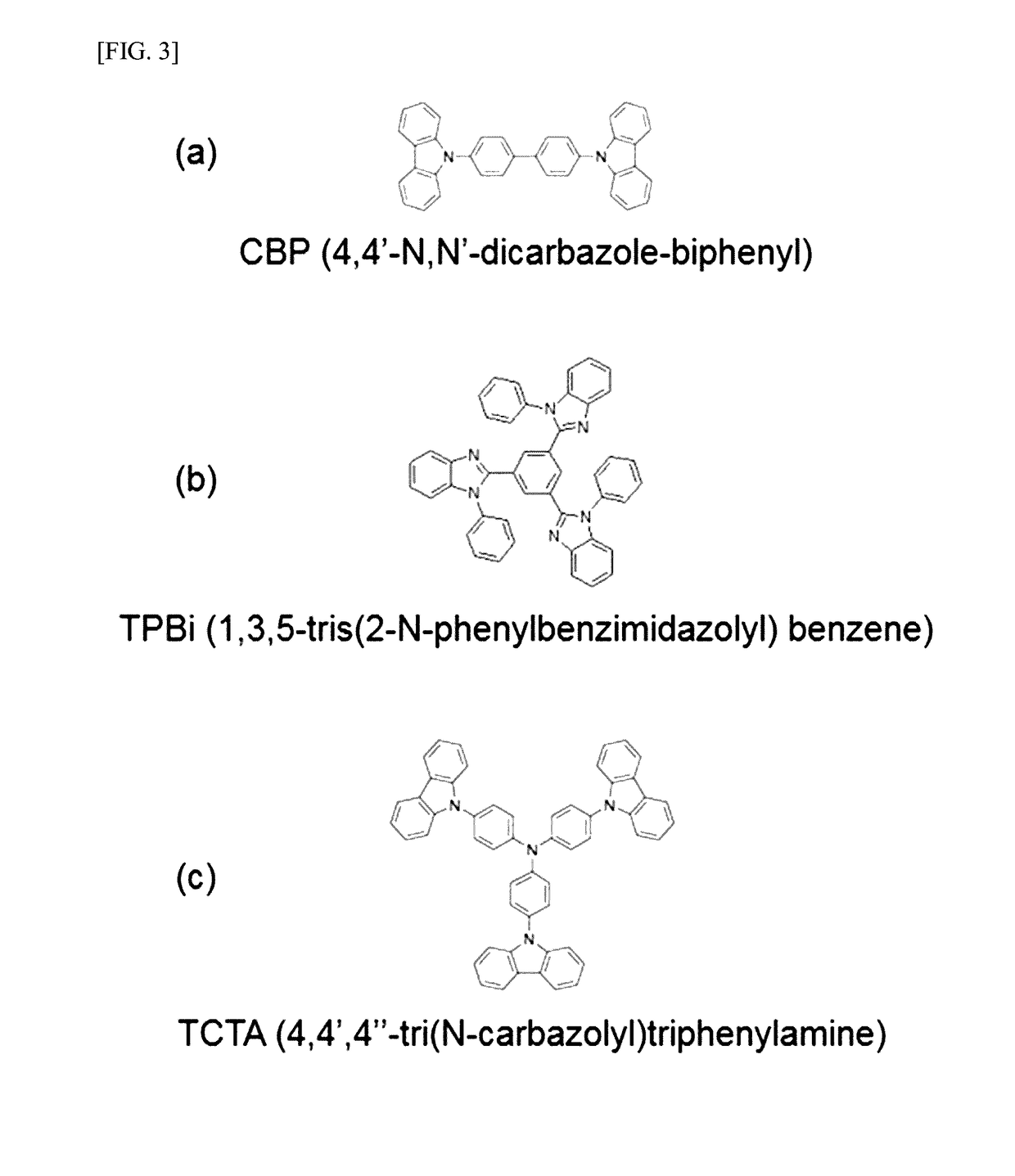
[0090]Next, TPBI was dissolved in chloroform at 0.03% by weight to prepare a TPBI solution.

[0091]Then, a conductive polymer material, PEDOT:PSS:PFI (a weight ratio of 1:6:25.4), was spin-coated with the CH3NH3PbBr3 solution thereon. The spin coating was continued by dripping the TPBI solution at 65 seconds after starting the spin-coating to form a CH3NH3PbBr3 layer in which the low-molecular-weight organic substance was included.

example 2

[0092]Formation of a Metal Halide Perovskite Light Emitting Layer Through Coating by Dripping a Low-Molecular-Weight Organic Substance Solution (an Organic-Substance-Assisted Nanocrystal Fixing Process)

[0093]A metal halide perovskite light emitting layer was formed in the same manner as in Example 1, except that TCTA was used as a low-molecular-weight organic substance instead of TPBI.

example 3

[0094]Formation of a Metal Halide Perovskite Light Emitting Layer Through Coating by Dripping a Low-Molecular-Weight Organic Substance Solution (an Organic-Substance-Assisted Nanocrystal Fixing Process)

[0095]A metal halide perovskite light emitting layer was formed in the same manner as in Example 1, except that CBP was used as a low-molecular-weight organic substance instead of TPBI.


PUM

PropertyMeasurementUnit
full width at half maximumaaaaaaaaaa
exciton diffusion lengthaaaaaaaaaa

Abstract

Provided are a metal halide perovskite light emitting device and a method of manufacturing the same. The method of manufacturing a metal halide perovskite light emitting device includes preparing a substrate having a positive electrode formed on an upper part thereof, starting coating the substrate on which the positive electrode is formed with a metal halide perovskite light emitting layer, forming a metal halide perovskite light emitting layer by dripping a low-molecular-weight organic substance solution during the coating of the metal halide perovskite light emitting layer, and forming a negative electrode on the light emitting layer. According to the present invention, a low-molecular-weight organic substance is included in a metal halide perovskite light emitting layer to reduce the sizes of grains in metal halide perovskites, to improve electrical characteristics by the effect of defect passivation on a metal halide perovskite, and to improve luminous efficiency of a thin film by reducing an exciton diffusion length by spatially trapping excitons well in decreased grains, thereby effectively improving efficiency of a metal halide perovskite light emitting diode and overcoming limitations in application.

Description

CROSS-REFERENCE TO RELATED APPLICATION[0001]This application claims priority to and the benefit of Korean Patent Application No. 10-2015-0152553, filed on Oct. 30, 2015, the disclosure of which is incorporated herein by reference in its entirety.BACKGROUND[0002]1. Field of the Invention[0003]The present invention relates to a metal halide perovskite light emitting device and a method of manufacturing the same, and more particularly, to a metal halide perovskite light emitting device having improved luminous efficiency, and a method of manufacturing the same.[0004]2. Discussion of Related Art[0005]In recent years, the display industry has been changed from inorganic light emitting diodes (LEDs) to organic light emitting diodes. The organic light emitting diodes have characteristics such as a relatively simple and lightweight structure and processability as well as a flexibility, and thus have come into the spotlight as next-generation flexible electronic devices. Meanwhile, inorganic...

Claims


Application Information

Patent Timeline
Patent Type & Authority Applications(United States)
IPC IPC(8): H01L51/56H01L51/00C09K11/06H01L51/50
CPCH01L51/56H01L51/5072H01L51/0007C09K11/06H01L51/5012H01L51/0035H01L51/0077C09K2211/188H01L51/0061H01L51/0072H01L51/0037H01L51/5016H10K50/115H10K71/00H10K50/16H10K71/15H10K50/11H10K85/30H10K85/111H10K85/636H10K85/1135H10K85/6572H10K2101/10
Inventor LEE, TAE-WOOPARK, MINHO
Owner POSTECH ACAD IND FOUND
Why Eureka
Try Eureka