Manufacture method for fullerence / PEDOT:PSS mixed solution and manufacture method for compound transparent conductive film having fullerence / PEDOT:PSS

a manufacturing method and technology of conductive film, applied in the field of display manufacture, can solve the problems of limiting the application of flexible panel and wearable device, and achieve the effect of cheap prices

Active Publication Date: 2017-06-01
TCL CHINA STAR OPTOELECTRONICS TECH CO LTD
View PDF3 Cites 1 Cited by
  • Summary
  • Abstract
  • Description
  • Claims
  • Application Information

AI Technical Summary

Benefits of technology

[0006]An object of the present invention is to provide a manufacture method of fullerence / PEDOT:PSS mixed solution, and then making fullerence / PEDOT:PSS mixed solution to manufacture a transparent conductive film; sources of applicable materials are broad and prices thereof are cheap; the fullerence / PEDOT:PSS mixed solution can be further utilized to manufacture a compound transparent conductive film having fullerence / PEDOT:PSS.

Problems solved by technology

However, because it takes a long time in the manufacturing process, the resistance of the ITO is higher, and the film cannot show the bending characteristic at a certain external force according to physical properties of the ITO film thereof; therefore, it limits the applications in flexible panel and wearable device as well.

Method used


Image

  • Manufacture method for fullerence / PEDOT:PSS mixed solution and manufacture method for compound transparent conductive film having fullerence / PEDOT:PSS
  • Manufacture method for fullerence / PEDOT:PSS mixed solution and manufacture method for compound transparent conductive film having fullerence / PEDOT:PSS

Examples


embodiment 1

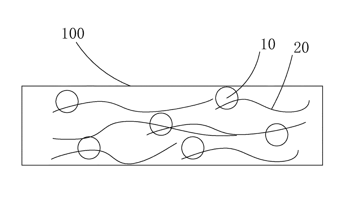
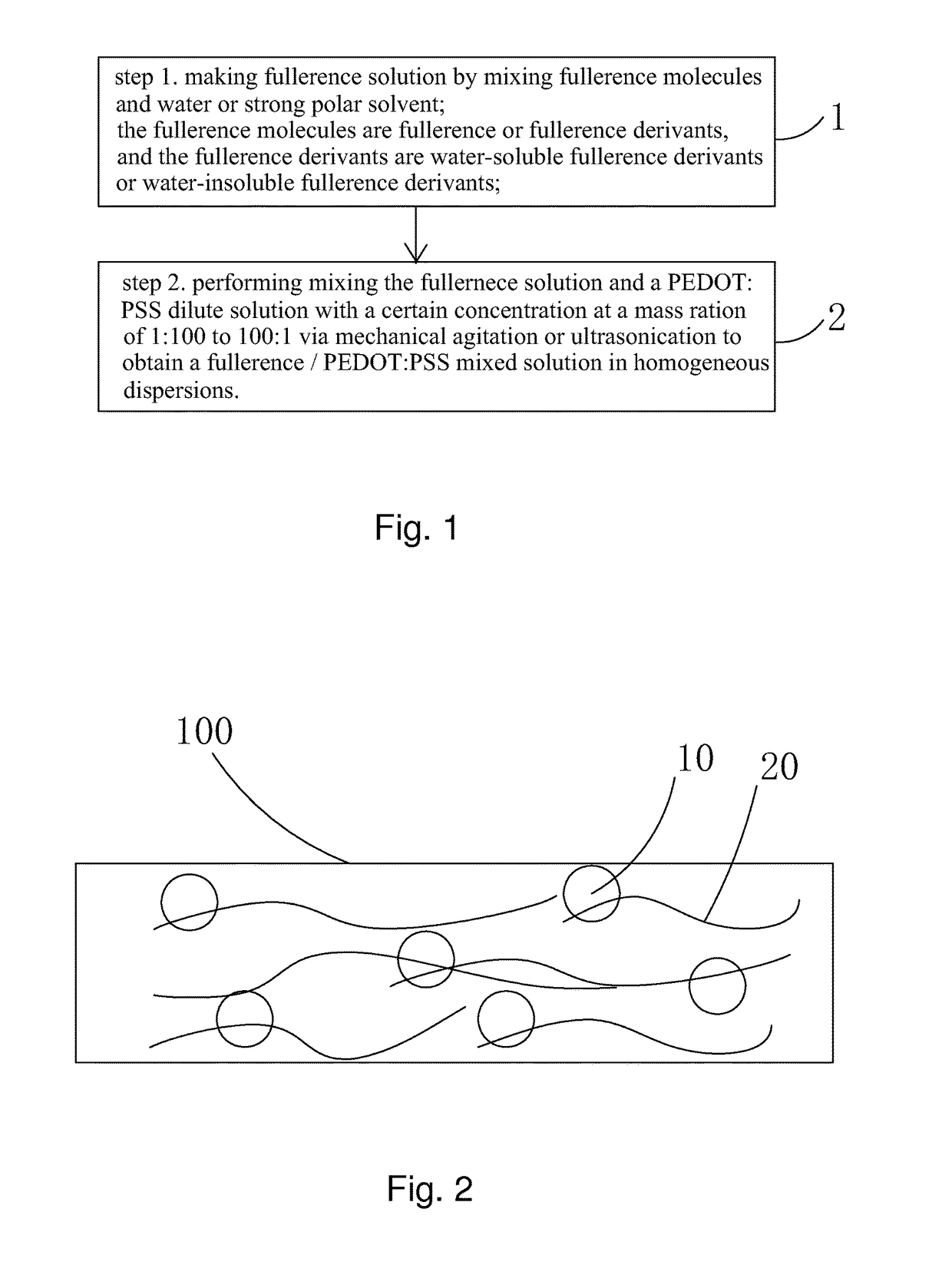
[0074]the manufacture method for compound transparent conductive film having fullerence / PEDOT:PSS of the present invention:

[0075]step 1. according to water-soluble fullerence derivants C60(OH)24 and deionized water at a mass ratio of 1:100, inserting the water-soluble fullerence derivants C60(OH)24 into the deionized water and performing ultrasound dispersion with 500 W ultrasonic power and 120 min ultrasonic time for obtaining homogeneous dispersions thereof to gain fullerence aqueous dispersions in homogeneous despersions, performing filtration to the fullerence aqueous dispersions to remove large particle aggregates to gain the fullerence solution, and then measuring the actual concentration thereof via spectrophotometry; the concentration of the water-soluble fullerence derivants C60(OH)24 in the fullerence solution is 6 mg / ml.

[0076]Step 2. performing mixing the fullernece solution and a PEDOT:PSS dilute solution with a certain concentration at a mass ration of 1:100 via mechani...

embodiment 2

[0082]the manufacture method for compound transparent conductive film having fullerence / PEDOT:PSS in the present invention:

[0083]step 1. according to water-insoluble fullerence derivants C60Br24, sodium dodecyl benzene sulfonate and deionized water at a mass ratio of 1:50:9050 to insert the fullerence or the water-insoluble fullerence derivants C60Br24 and sodium dodecyl benzene sulfonate into the deionized water and performing mechanical agitation for obtaining homogeneous dispersions thereof to gain fullerence aqueous dispersions, performing centrifugation with 5000 rpm of centrifugation and 5 min of the centrifugation time to the fullerence aqueous dispersions for removing large particle aggregates to gain the fullerence solution, and then measuring the actual concentration thereof via spectrophotometry; the concentration of the water-insoluble fullerence derivants C60(OH)24 in the fullerence solution is 0.05 mg / ml;

[0084]step 2. performing mixing the fullernece solution and a PED...

embodiment 3

[0090]the manufacture method for compound transparent conductive film having fullerence / PEDOT:PSS in the present invention:

[0091]step 1. according to fullerence C60 and strong polar solvent at a mass ratio of 1:200 to insert the fullerence C60 into N,N′-dimethyl formamide and performing ultrasound dispersion with 900 W ultrasonic power and 10 min ultrasonic time for obtaining homogeneous dispersions thereof to gain fullerence aqueous dispersions, performing centrifugation to the fullerence aqueous dispersions to remove large particle aggregates to gain the fullerence solution, and then measuring the actual concentration thereof via spectrophotometry; the concentration of the fullerence solution C60 in the fullerence solution is 3 mg / ml.

[0092]Step 2. performing mixing the fullernece solution and a PEDOT:PSS solution with a certain concentration at a mass ration of 100:1 via mechanical agitation or ultrasonication to obtain a fullerence / PEDOT:PSS mixed solution in homogeneous dispersi...


PUM

PropertyMeasurementUnit
concentrationaaaaaaaaaa
temperatureaaaaaaaaaa
ultrasonic timeaaaaaaaaaa

Abstract

A manufacture method for fullerence/PEDOT:PSS mixed solution and a manufacture method for compound transparent conductive film having fullerence/PEDOT:PSS are provided in the present invention: making fullerence/PEDOT:PSS mixed solution to manufacture a transparent conductive film; sources of applicable materials are broad and prices thereof are cheap; the fullerence/PEDOT:PSS mixed solution can be further utilized to manufacture a compound transparent conductive film having fullerence/PEDOT:PSS on substrates or a variety of devices; the present invention discloses a manufacture method for a compound transparent conductive film having fullerence/PEDOT:PSS, and when manufacturing the compound transparent conductive film having fullerence/PEDOT:PSS via wet coating process which is with low cost and high efficiency comparing with manufacture of ITO film, and furthermore expensive PVD equipment can be waived, production cost can be reduced, manufacturing method can be simplified at the same time, production time is shorter and economic efficiency can be increased; the compound transparent conductive film having fullerence/PEDOT:PSS manufacturing in the present invention has high conductivity and high light transmittance to replace ITO films in the market.

Description

TECHNICAL FIELD[0001]The present invention relates to a display manufacture filed, in particular to a manufacture method for fullerence / PEDOT:PSS mixed solution and a manufacture method for compound transparent conductive film having fullerence / PEDOT:PSS.BACKGROUND[0002]In display technical field, a flat panel display as a liquid crystal display (LCD), an organic light emitting diode(OLED), and so forth is gradually substituted for cathode ray tube (CRT) monitor, and are applied to the liquid crystal display television, cell phone, personal digital assistant, calculator panel, or laptop panel.[0003]A display panel is an important part of LCD or OLED; take LCD for example: the display panel is mainly composed of a thin film transistor (TFT) substrate, a color filter (CF) substrate, and a liquid crystal layer between the thin film transistor substrate and the color filter substrate; the working principles is that a driving voltage is applied to an transparent conductive electrode on t...

Claims


Application Information

Patent Timeline
Patent Type & Authority Applications(United States)
IPC IPC(8): C08J3/07C09D125/06C09D7/12B05D3/04H01L51/00C08J3/215B05D1/02C09D165/00C09D5/24C09D7/61
CPCC08J2365/00C09D165/00G02F1/13439C09D125/06C09D7/1216C09D5/24H01L51/0037H01L51/004H01L51/0046C08J3/215B05D1/02B05D3/0406C08J2325/06C08J3/07H01L51/0021C08J5/18C08L65/00C09D125/18C08L25/18C08G2261/1424C08G2261/3223C08G2261/794C08J2325/18C08J2465/00G02F2202/022G02F2202/16C08K3/045H01B1/04H01B1/127C09D7/61H10K71/12H10K71/60H10K85/211H10K85/1135H10K10/82H10K30/81H10K50/81H10K85/141
Inventor HU, TAOWU, YUE
Owner TCL CHINA STAR OPTOELECTRONICS TECH CO LTD
Why Eureka
Try Eureka