

Process for manufacturing nickel oxide films with high conductivity
Inactive Publication Date: 2017-06-08
MING CHI UNIVERSITY OF TECHNOLOGY
View PDF2 Cites 3 Cited by
- Summary
- Abstract
- Description
- Claims
- Application Information
AI Technical Summary
Benefits of technology
This is a new process for making high-conductivity nickel oxide films using a special type of sputtering system called HIPIMS. This system produces a high-density plasma that can ionize atoms in the film, resulting in a larger amount of Ni3+ ions and higher conductivity of the p-type NiO film. Compared to traditional methods, this process has a higher sputtering power, resulting in improved performance of the nickel oxide film.
Problems solved by technology
However, the traditional magnetron sputtering process has a low sputtering power that may cause low ionization (that is, less Ni3+ ions), and therefore it would be difficult to develop NiO films with high conductivity.
Method used
View moreImage
Smart ImageViewing Examples

Examples
embodiments
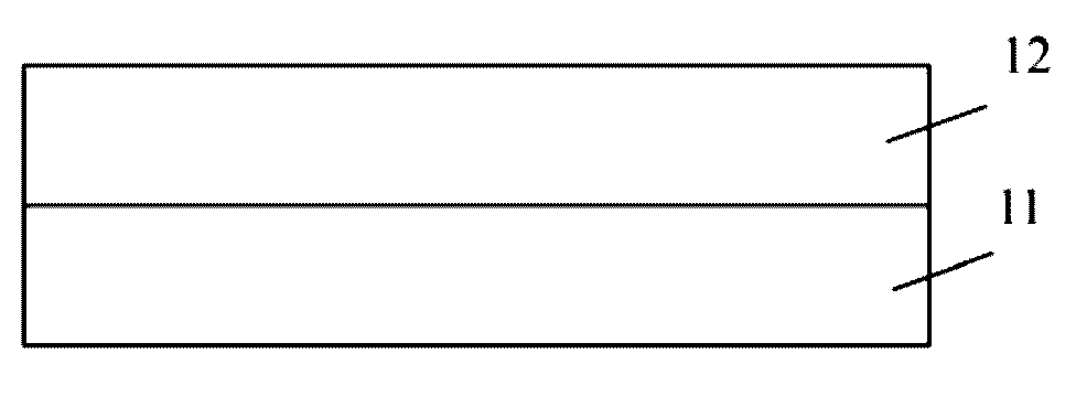
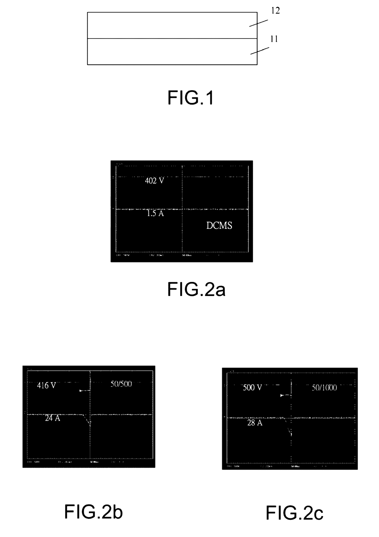
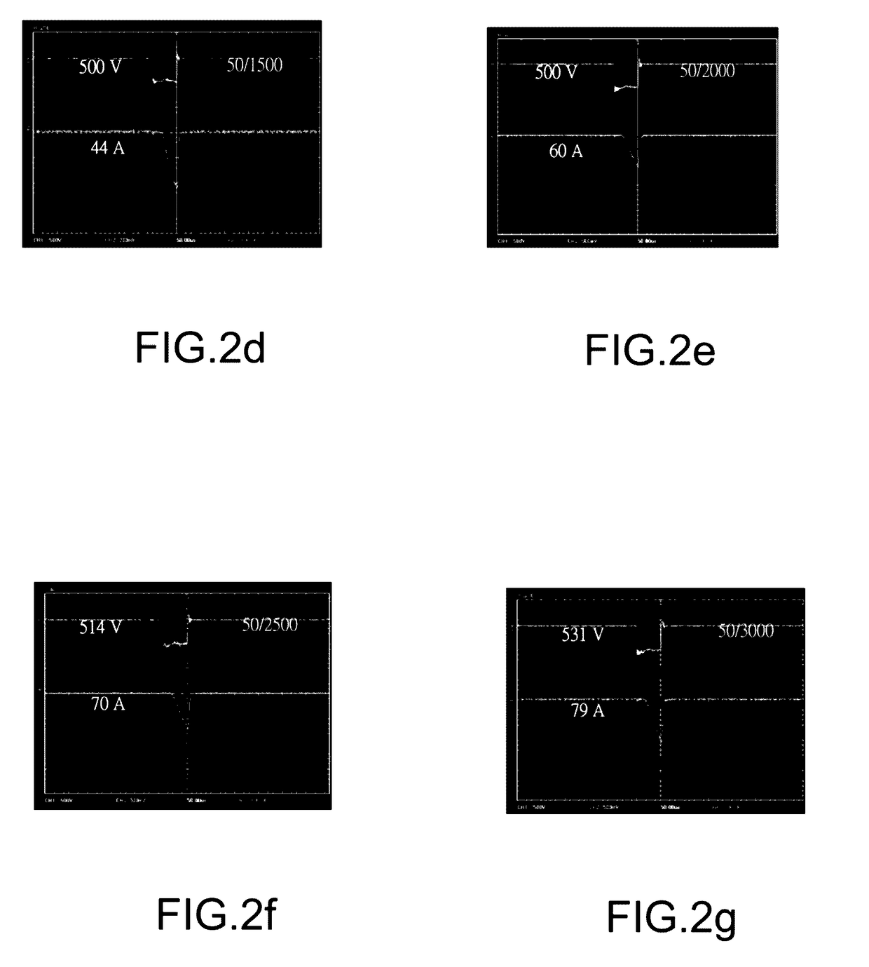
[0033]NiO film with a thickness of 100 nm is formed on a substrate, for example glass and Si substrate with a reactive magnetron sputtering process by high power impulse magnetron sputtering system, HIPIMS system sputtering Ni target. The power source of HIPIMS is a pulse generator fed with a DC power source. In the embodiment, NiO film is deposited with different duty cycles.
Login to View More PUM
| Property | Measurement | Unit |
|---|---|---|
| Thickness | aaaaa | aaaaa |
| Surface energy | aaaaa | aaaaa |
| Electrical conductor | aaaaa | aaaaa |
Abstract
The invention provides a process for manufacturing nickel oxide films with high conductivity, comprising steps of: operating a high power impulse magnetron sputtering system, HIPIMS system, in an argon and oxygen mixture, at peak power density higher than 1000 W / cm2 under a low duty cycle; and sputtering a Ni target to form the p-type NiO film with high conductivity on a substrate, the duty cycle=ton / (ton+toff), wherein ton is time of pulse on and toff is time of pulse off.
Description
BACKGROUND OF THE INVENTION[0001]Field of the Invention[0002]The present invention relates to a process for manufacturing transparent conductive oxide films, more particularly to a process for manufacturing nickel oxide films.[0003]Description of the Prior Art[0004]Most of transparent conductive oxide (TCO) films semiconductor material.[0005]They may be divided into two types, one type of p-type TCO and another type of n-type TCO. The n-type TCO process was developed earlier and is an established technology. Nowadays, indium tin oxide (ITO) has been commercial products in the industry that belongs to the n-type TCO. However, in the application of opto-electronic components such as diodes and transistors, developing a highly conductive p-type TCO films is an important research topic. In some researches, it has been found NiO, CuAlO2, ZnO:N, Cu2O and SrCu2O2 have potential as a p-type TCO, wherein NiO film has a wide band gap range (3.6-4.0 eV), high dielectric constant (S˜11.9), anti...
Claims
Login to View More Application Information
Patent Timeline
 IPC IPC(8): C23C14/34C23C14/08H01J37/34C23C14/35
CPCC23C14/3414C23C14/35C23C14/3485H01J37/3426C23C14/085H01J37/3467H01J37/3405C23C14/3457C23C14/0036H01J37/3491
InventorCHEN, SHENG-CHIKUO, TSUNG-YENLIN, HSIN-CHIH
OwnerMING CHI UNIVERSITY OF TECHNOLOGY