Cleaning device for atomizing and spraying liquid in two-phase flow

a cleaning device and two-phase flow technology, applied in the direction of spraying apparatus, moving spraying apparatus, electrical apparatus, etc., can solve the problems of increasing the difficulty of removing contaminants with a smaller size on the wafer surface by using the conventional single-wallet wet cleaning process, extreme waste of resources, and large atomized particles produced by the current cleaning device, etc., to improve the uniformity of ultrasonic or megasonic energy applied to the wafer surface, uniform gas flow distribution, and improved

Active Publication Date: 2017-06-15
BEIJING NAURA MICROELECTRONICS EQUIP CO LTD
View PDF3 Cites 15 Cited by
  • Summary
  • Abstract
  • Description
  • Claims
  • Application Information

AI Technical Summary

Benefits of technology

[0041]6. A gas separating plate can be provided in the gas intake pipeline to achieve a uniform gas flow distribution, and improve the size and amount distribution uniformity of the atomized particles.
[0042]7. The cleaning liquid with the ultrasonic or megasonic energy can be atomized by the cleaning device to form the atomized particles. Since these atomized particles are randomly distributed into the cleaning liquid membrane on the wafer surface both in time and in space, the ultrasonic or megasonic energy carried by the atomized particles will not generate a stable energy interference field. In other words, the uniformity of the ultrasonic or megasonic energy applied to the wafer surface is improved, so as to effectively suppress the damage to the patterns on the wafer surface.
[0043]8. Compared with the conventional cleaning device, the cleaning device of the present invention with the ultrasonic or megasonic oscillation means can spray the atomized particles with ultrasonic or megasonic energy into the cleaning liquid membrane on the wafer surface. Accordingly, in addition that the atomized particles injected to the wafer surface with the kinetic energy forms a shock wave in the liquid membrane, the ultrasonic or megasonic energy is also carried into the liquid membrane by the atomized particles to form a shock wave due to the collapse of cavitation bubbles or a straight flow, thus to improve the efficiency of removing the contaminants on the wafer surface, shorten the process time, save the usage of the cleaning liquid and the high-purity gas, reduce the production cost, and decrease the influence for the environment.
[0044]9. In the two-phase flow cleaning process, a shielding gas can be sprayed out from the shielding gas outlet at an inclined angle and forms a gas shielding layer above the wafer, which prevents the reaction between the silicon element on the wafer surface and the oxygen in the cleaning chamber. In the drying process, the liquid intake pipeline can be turned off while keeping the gas intake pipeline and the shielding gas outlet both opened to replace the conventional single spray arm which injects a drying gas individually, so as to perform a rapid drying process to the entire wafer surface including

Problems solved by technology

However, with the critical dimension of the integrated circuit patterns scaling down, it becomes increasingly difficult to remove the contaminants with a smaller size on the wafer surface by using the conventional single wafer wet cleaning process.
However, the atomized particles produced by the current cleaning device have larger size and higher energy, which is prone to cause problems such as the damage to the surface pattern when being applied in the wafer cleaning process under sub-65 nm and beyond technology.
On the other hand, the low utilization of the liquid flow in the conventional cleaning device also leads to an extreme waste of resources.
On the other hand, with the continuous progress of the semiconductor IC manufacturing technology, the size of the semiconductor device is becoming smaller and smaller, as a result, micro particles may be enough to affect the manufacturing process and the performance of the semiconductor device.
However, the traditional fluid cleaning method cannot effectively remove these micro particles due to a relatively static boundary layer that formed between the wafer surface and the cleaning liquid.
Although the ultrasonic or megasonic cleaning process can improve the removing efficiency of the contaminants, the damage to the patterns on the wafer surface still occurs.
Specifically, since the ultrasonic or megasonic energy is propagated in the liquid medium through waves, regions of high ultrasonic or megasonic energy density are formed at specific positions where wave superposition is generated and air bubbles have much higher energy when collapsed than the strength of the pattern structures on the wafer surface, which causes the damage to the patterns.
Furthermo

Method used


Image

  • Cleaning device for atomizing and spraying liquid in two-phase flow
  • Cleaning device for atomizing and spraying liquid in two-phase flow
  • Cleaning device for atomizing and spraying liquid in two-phase flow

Examples


Embodiment Construction

[0068]The present invention will be described in further details hereinafter by referring to the accompanying drawings, so as to provide a better understanding of the present invention.

[0069]It should be noted that, in the following specific embodiments, when these embodiments of the present invention are described in detail, in order to clearly illustrate the structure of the present invention to facilitate explanation, the accompanying drawings are not necessarily drawn to scale, some features in the drawings may have been fragmentary enlarged, deformed or simplified. Therefore, it should be avoided to understand this as a limitation to the present invention.

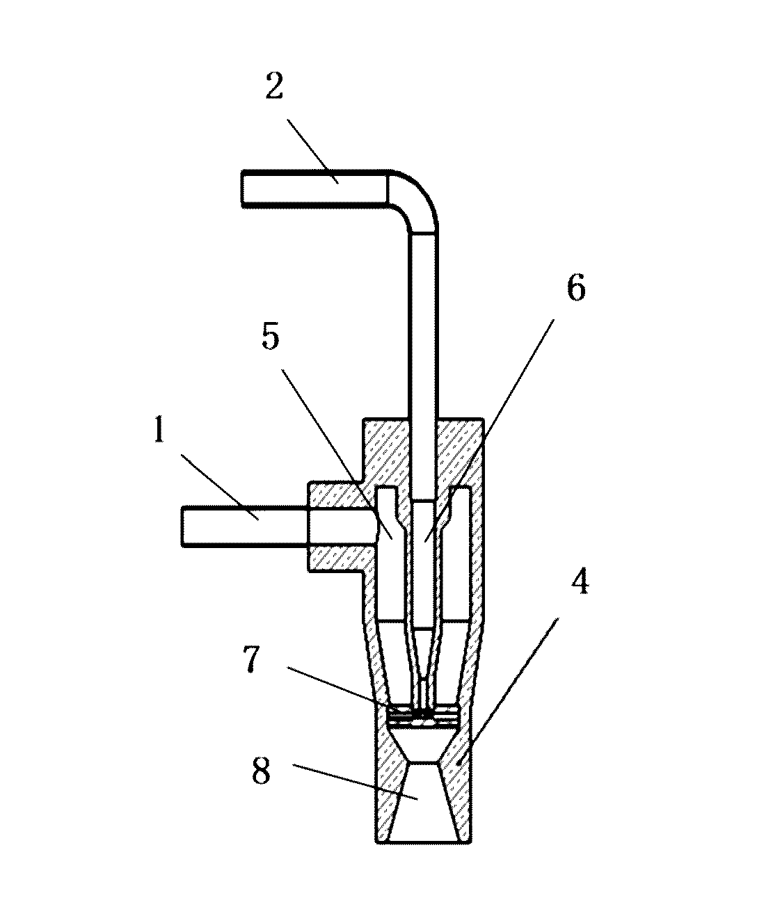
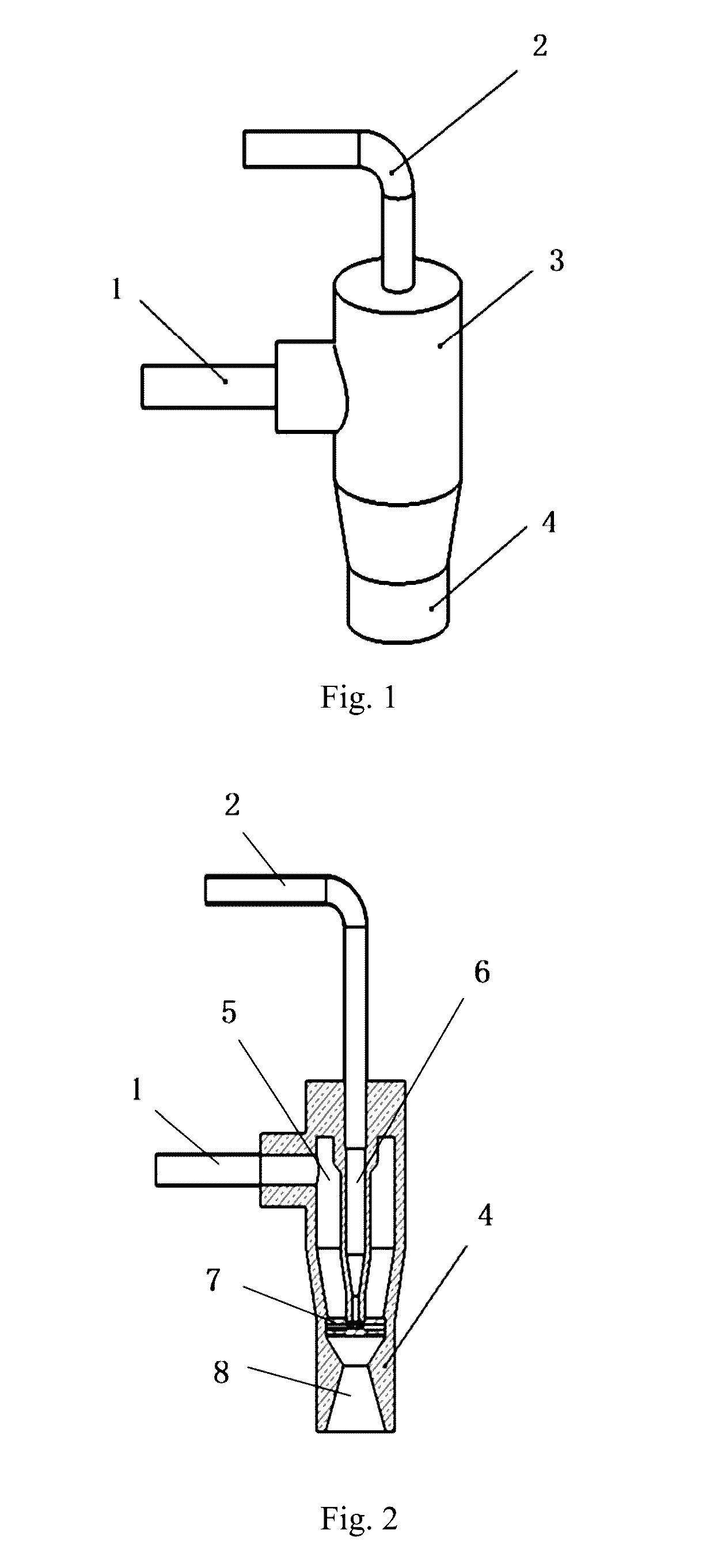
[0070]Referring to FIGS. 1˜2, which are schematic views illustrating a cleaning device for atomizing and spraying liquid in two-phase flow having a round-shaped nozzle according to a preferred embodiment of the present invention. As shown in FIG. 1, which discloses an outline structure of the cleaning device according to the p...


PUM


Abstract

A cleaning device for atomizing and spraying liquid in two-phase flow comprising a nozzle provided with multiple liquid bypass pipelines each having liquid guiding outlets inclined at a predetermined angle and an exhaust mesh plate having vertical gas guiding outlets, which makes the high speed liquid flow and high speed gas flow sprayed out therefrom collide against each other sufficiently to form ultra-micro atomized particles with uniform and adjustable size. The ultra-micro atomized particles are sprayed out downwardly to the wafer surface under the acceleration and vertical orientation effects of an atomized particle guiding outlet to perform a reciprocating cleaning for the wafer. Other components such as an ultrasonic or megasonic generation unit, a gas shielding unit, a self-cleaning unit or a rotating unit can also be provided to perform the multifunction of the nozzle.

Description

CROSS-REFERENCE TO RELATED APPLICATION[0001]This application claims the priority benefit of China patent application serial No. 201521027544.3, No. 201521028786.4, No. 201521027568.9, and No. 201521028612.8, filed Dec. 10, 2015. The entirety of each of the above-mentioned patent applications are hereby incorporated by reference herein and made a part of the specificationsFIELD OF THE INVENTION[0002]The present invention relates to the field of semiconductor cleaning technology, and particularly to a cleaning device for atomizing and spraying liquid in two-phase flow.BACKGROUND OF THE INVENTION[0003]With the rapid development of the semiconductor IC manufacturing technology, the pattern critical dimension of the integrated circuit chips has scaled down to the deep sub micrometer stage, and accordingly the dimension of the main contaminants (such as particles) which will cause the failure or damage to the ultra-fine circuits on the chip also greatly decreases.[0004]In the IC manufactu...

Claims


Application Information

Patent Timeline
IPC IPC(8): H01L21/67B05B7/04B05B3/08B05B15/02B05B13/02B05B17/06B05B15/04
CPCH01L21/67051B05B17/0607B05B7/045B05B3/085B05B15/025B05B13/0278B05B15/0437B05B7/0466B05B15/55
Inventor TENG, YULI, WEI
Owner BEIJING NAURA MICROELECTRONICS EQUIP CO LTD
Why Eureka
Try Eureka