Carrier-free semiconductor package and fabrication method

a carrier-free, semiconductor technology, applied in semiconductor devices, semiconductor/solid-state device details, electrical devices, etc., can solve the problems of poor adhesion, inability to further reduce the height of the entire qfn semiconductor package, and limited by the encapsulant thickness, so as to avoid transportation difficulty occurring to a conventional weak and pliable copper plate, increase the adhesion, and improve the adhesion

Active Publication Date: 2017-07-13
SILICONWARE PRECISION IND CO LTD
View PDF5 Cites 2 Cited by
  • Summary
  • Abstract
  • Description
  • Claims
  • Application Information

AI Technical Summary

Benefits of technology

[0010]In view of the above drawbacks of the prior art, it is an object of the present invention to provide a carrier-free semiconductor package and a fabrication method thereof so as to avoid the use of costly metals such as gold and palladium as an etching resist layer, thereby reducing the fabrication cost.
[0011]Another object of the present invention is to provide a carrier-free semiconductor package and a fabrication method thereof so as to prevent delamination of a plating layer from an encapsulant.
[0012]A further object of the present invention is to provide a carrier-free semiconductor package and a fabrication method thereof so as to prevent solder pads from dropping from an encapsulant during rework of the semiconductor package.
[0013]Still another object of the present invention is to provide a carrier-free semiconductor package and a fabrication method thereof so as to avoid warpage and transportation difficulty of a copper plate.
[0014]A further object of the present invention is to provide a carrier-free semiconductor package and a fabrication method thereof, which allows a plurality of conductive traces to be flexibly disposed on a copper carrier so as to effectively shorten the arc length of bonding wires electrically connecting a chip and the conductive traces, thereby enhancing the circuit routability and electrical connection quality of the semiconductor package.
[0025]Therefore, the carrier-free semiconductor package and a method for fabricating the same of the present invention uses a half-etching method to form on a metal carrier a plurality of recess grooves and metal studs each serving as a die pad or a solder pad, and fills the recess grooves with a first encapsulant such that the first encapsulant is directly attached to the metal carrier (metal studs) made of a material such as copper to thereby enhance the adhesion between the first encapsulant and the metal carrier (metal studs) and to overcome the conventional drawback of dropping of solder pads from an encapsulant during rework of a semiconductor package. The present invention further forms an antioxidant layer such as a silver plating layer or an OSP film on the upper surfaces of the metal studs and performs die-bonding, wire-bonding and molding processes respectively to form a second encapsulant encapsulating the chip. Since the half-etched recess grooves filled up by the first encapsulant add structural strength to the overall metal carrier, transportation difficulty occurring to a conventional weak and pliable copper plate is avoided. Further, the invention eliminates the use of costly metals such as gold and palladium as an etching resist layer to reduce the fabrication cost of the semiconductor package, and further allows a plurality of conductive traces to be flexibly disposed on the metal carrier to enhance the electrical connection quality of the semiconductor package.

Problems solved by technology

However, limited by encapsulant thickness, the entire height of the QFN semiconductor packages cannot be further reduced to follow the trend of developing thinner and lighter semiconductor devices.
However, the thickness of the electroplated solder pads 12 is only about 1 to 5 μm and the electroplated solder pads 12 has a poor adhesion with the encapsulant 15, which easily leads to a problem of delamination between the electroplated solder pads 12 and the encapsulant 15 and even causes cracking of the bonding wires 14.
Further, a costly metal such as gold or palladium is required to form an etching resist layer when the copper plate is removed by etching, thereby increasing the fabrication cost.
However, since the nickel or silver layer has a poor adhesion with the encapsulant, delamination is easy to occur therebetween under a thermal stress so as to cause permeation of moisture.
Furthermore, since die-bonding, wire-bonding and molding processes are respectively performed on the half-etched copper, the thickness of the half-etched copper plate has been reduced by half, and thus the half-etched copper plate is so weak and pliable that it is not suitable for transportation and warpage of the copper plate easily occurs under a thermal effect.
Moreover, as I / O count increases, wire crossing can easily occur to the array-arranged solder pads 22, thereby resulting in a problem of short circuit.

Method used


Image

  • Carrier-free semiconductor package and fabrication method
  • Carrier-free semiconductor package and fabrication method
  • Carrier-free semiconductor package and fabrication method

Examples


first embodiment

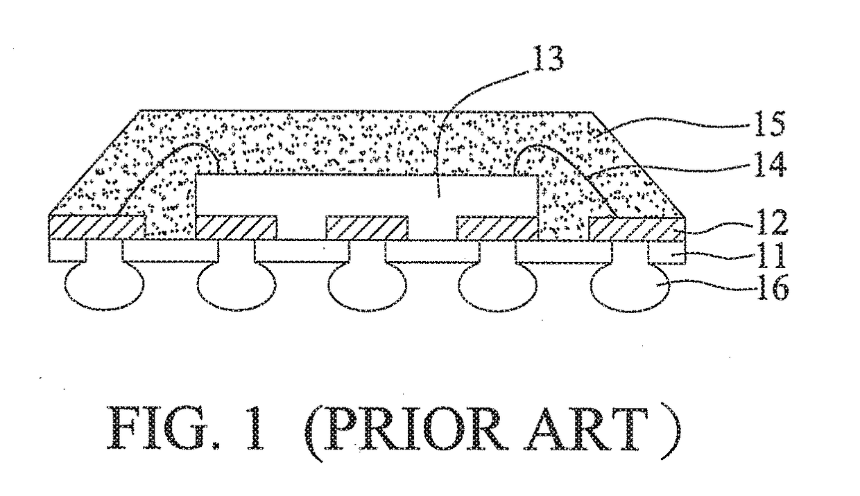
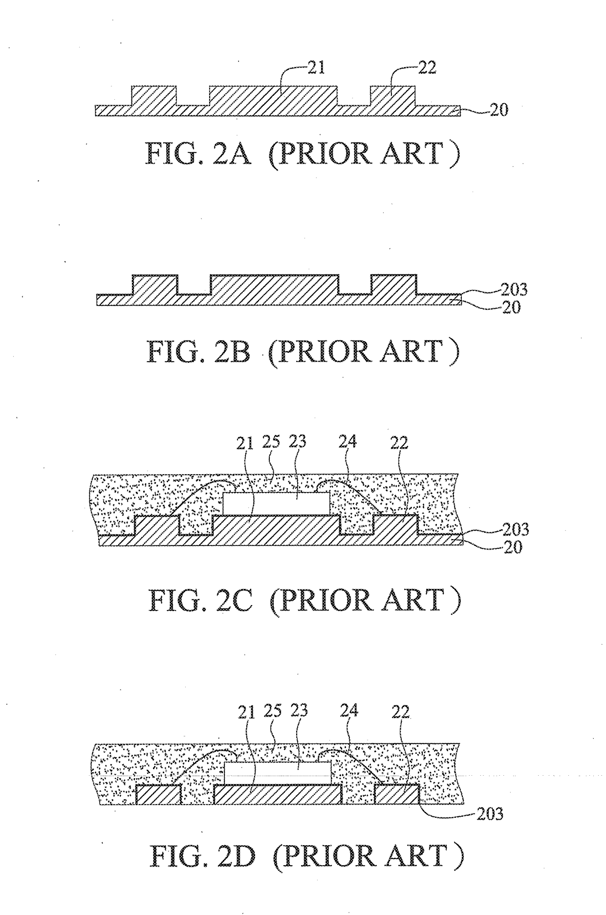
[0035]FIGS. 3A to 3G show a carrier-free semiconductor package and a fabrication method thereof according to a first embodiment of the present invention. Referring to FIG. 3A, a metal carrier 30 such as a copper plate is prepared, which has a first surface 30a and an opposite second surface 30b. Referring to FIG. 3B, a patterned first resist layer 31a is formed on the first surface 30a of the metal carrier 30 so as to define positions of die pads and solder pads, and a second resist layer 31b is formed to cover the second surface 31b of the metal carrier 30. Referring to FIG. 3C, a part of the metal carrier 30 not covered by the first resist layer 31a is removed through a half-etching process so as to form a plurality of recess grooves 301 and metal studs 302 on the first surface 31a of the metal carrier 30. Then, the first resist layer 31a and the second resist layer 31b are removed. The metal studs 302 serve as solder pads 302a and die pads 302b, respectively. Referring to FIG. 3D...

second embodiment

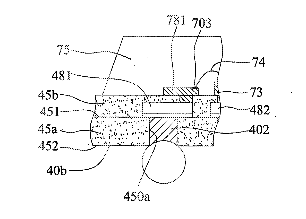
[0042]FIGS. 4A to 4D show a carrier-free semiconductor package and a fabrication method thereof according to a second embodiment of the present invention.

[0043]The present embodiment is similar to the first embodiment. A main difference of the present embodiment from the first embodiment is that conductive traces are further formed on the top surface of the first encapsulant and the upper surfaces of the metal studs and electrically connected to the metal studs.

[0044]Referring to FIG. 4A, as in the first embodiment, a plurality of recess grooves 401 and metal studs 402 are formed on a first surface of a metal carrier 40, the recess grooves 401 are filled with a first encapsulant 45a and the upper surfaces of the metal studs 402 are exposed from the first encapsulant 45a. Then, a conductive layer 47 such as a thin copper layer is formed on the top surface of the first encapsulant 45a and the upper surfaces of the metal studs 402 by electroless plating or sputtering.

[0045]Referring to...

third embodiment

[0049]FIG. 5 shows a carrier-free semiconductor package and a method for fabricating the same according to a third embodiment of the present invention.

[0050]The present embodiment is similar to the above embodiment. A main difference of the present embodiment from the above embodiment is that a semiconductor chip is electrically connected to the terminals of conductive traces via solder bumps in a flip-chip manner.

[0051]Referring to FIG. 5, a semiconductor chip 53 is disposed on conductive traces 581 in a flip-chip manner. In particular, the active surface of the semiconductor chip 53 is faced towards the conductive traces 581 and electrically connected to the terminals of the conductive traces 581 through a plurality of solder bumps 59 during the die bonding process.

[0052]Compared with a wire bonding packaging structure for connecting the semiconductor chip and the conductive traces, the flip chip packaging structure shortens the electrical connection path between the semiconductor...


PUM

PropertyMeasurementUnit
thicknessaaaaaaaaaa
thicknessaaaaaaaaaa
conductiveaaaaaaaaaa

Abstract

A method for fabricating a carrier-free semiconductor package includes: half-etching a metal carrier to form a plurality of recess grooves and a plurality of metal studs each serving in position as a solder pad or a die pad; filing each of the recess grooves with a first encapsulant; forming on the metal studs an antioxidant layer such as a silver plating layer or an organic solderable protection layer; and performing die-bonding, wire-bonding and molding processes respectively to form a second encapsulant encapsulating the chip. The recess grooves are filled with the first encapsulant to enhance the adhesion between the first encapsulant and the metal carrier, thereby solving the conventional problem of having a weak and pliable copper plate and avoiding transportation difficulty. The invention eliminates the use of costly metals as an etching resist layer to reduce fabrication cost, and further allows conductive traces to be flexibly disposed on the metal carrier to enhance electrical connection quality.

Description

BACKGROUND OF THE INVENTION[0001]1. Field of the Invention[0002]The present invention relates generally to semiconductor packages and fabrication methods thereof, and more particularly, to a carrier-free semiconductor package and a fabrication method thereof.[0003]2. Description of Related Art[0004]Conventionally, there are various kinds of semiconductor packages that use lead frames as chip carriers. Therein, quad flat packages (QFPs) have outer leads for electrical connecting to external devices while quad flat non-leaded (QFN) semiconductor packages dispense with outer leads to reduce the package size. However, limited by encapsulant thickness, the entire height of the QFN semiconductor packages cannot be further reduced to follow the trend of developing thinner and lighter semiconductor devices. Therefore, carrier-free semiconductor packages are developed, which are much thinner and lighter than the conventional lead frame type semiconductor packages.[0005]FIG. 1 shows a carrier...

Claims


Application Information

Patent Timeline
Patent Type & Authority Applications(United States)
IPC IPC(8): H01L23/495H01L21/56H01L23/31H01L23/00H01L21/48H01L21/683
CPCH01L23/49582H01L21/4832H01L21/6835H01L23/3128H01L24/16H01L24/32H01L2224/73265H01L21/568H01L23/49548H01L2221/68345H01L2221/68377H01L2224/48091H01L2224/48247H01L24/48H01L2224/16225H01L2224/92247H01L2224/97H01L2924/01046H01L2924/01078H01L2924/01079H01L2924/15311H01L2924/181H01L2924/00014H01L2224/85439H01L2224/85H01L2924/3512H01L2924/00H01L2924/00012H01L2224/45099H01L2224/45015H01L2924/207
Inventor TSAI, YUEH-YINGTANG, FU-DIHUANG, CHIEN-PINGKE, CHUN-CHI
Owner SILICONWARE PRECISION IND CO LTD
Why Eureka
Try Eureka