System and method for micro-nano machining by femtosecond laster two-photon polymerization

a two-photon polymerization and micro-nano technology, applied can solve the problems of limited two-photon polymerization, limited further application of the technology in the field of micro-nano machining, and low machining efficiency, so as to improve the time for machining and forming for each layer, improve the and improve the effect of machining efficiency and the process flow

Active Publication Date: 2017-07-27
SOUTH UNIVERSITY OF SCIENCE AND TECHNOLOGY OF CHINA
View PDF3 Cites 8 Cited by
  • Summary
  • Abstract
  • Description
  • Claims
  • Application Information

AI Technical Summary

Benefits of technology

[0030]According to the system and method for the micro-nano machining by femtosecond laser two-photon polymerization, the image capture apparatus is arranged in a light path for the micro-nano machining by the femtosecond lasers, so that not only one beam of femtosecond lasers can be divided into a plurality of beams of parallel femtosecond lasers to realize simultaneous machining for a plurality of three-dimensional micro-nano devices, but also one-time projection forming for each layer of the cross-section graphs of the manufactured devices can be realized. Moreover, all layers of the cross-section graphs may be different. In this way, any complex three-dimensional micro-nano device can be machined, so as to greatly improve the machining efficiency and the process flow. Additionally, in the layer-by-layer micro-nano machining process, the displacement platform only needs to move along the direction of cross-section thickness of the micro-nano device and does not need to move point by point along the plane two-dimensional direction. In this way, the time for machining and forming for each layer of the cross sections of the three-dimensional micro-nano device is obviously shortened, the machining efficiency and the process flow are improved, and the positioning precision requirement in the plane two-dimensional direction is reduced, so that the machining process is simplified, and the difficulty is reduced.

Problems solved by technology

The technology utilizes the femtosecond lasers with longer wave length as the light source, laser beams are focused by a focusing objective lens on a light-sensitive material to be machined, and the light-sensitive material generates a polymerization reaction at a focal point through two-photon absorption action; however, two-photon absorption is not generated at other places of a light path due to lower laser intensity; meanwhile, a corresponding single-photon absorption process is not generated due to lower laser energy; and therefore, two-photon polymerization is only limited to the focal point.
Therefore, the machining for one three-dimensional micro-nano device requires a large amount of point polymerization processes, the time is longer, the machining efficiency is low, and the process flow is not sufficient to meet industrial production demands, causing a limit to further application of the technology in the field of the micro-nano machining.
However, the above method for multifocal parallel machining is more suitable for batch production of the micro-nano device with a periodic structure, but batch production of any complex three-dimensional device by the method is still highly difficult.
Therefore, the machining efficiency for any complex three-dimensional device is improved in a limited range by the existing method for multifocal parallel machining, and the high-precision mechanical positioning capability is required in a three-dimensional direction, increasing machining difficulty.

Method used


Image

  • System and method for micro-nano machining by femtosecond laster two-photon polymerization
  • System and method for micro-nano machining by femtosecond laster two-photon polymerization
  • System and method for micro-nano machining by femtosecond laster two-photon polymerization

Examples


embodiment 1

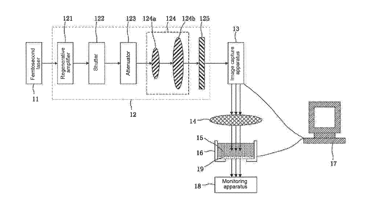
[0042]Embodiment 1 of the present disclosure provides a system for micro-nano machining by femtosecond laser two-photon polymerization. FIG. 1 is a schematic structural diagram illustrating the system for the micro-nano machining by femtosecond laser two-photon polymerization provided by the embodiment 1 of the present disclosure. As shown in FIG. 1, the system for the micro-nano machining by femtosecond laser two-photon polymerization includes: a femtosecond laser 11, configured to generate femtosecond lasers; an external light path modulation unit 12, configured to modulate the femtosecond lasers; an image capture apparatus 13, configured to capture cross-section graphs of a three-dimensional micro-nano device layer by layer, so that the modulated femtosecond lasers form parallel beams arranged according to all layers of the cross-section graphs; a focusing lens 14, configured to respectively focus the parallel beams arranged according to all layers of the cross-section graphs in ...

embodiment 2

[0049]Embodiment 2 of the present disclosure also provides a system for micro-nano machining by femtosecond laser two-photon polymerization. Based on the embodiment 1, the dynamic image capture apparatus is adopted as the image capture apparatus of the present embodiment.

[0050]In the present embodiment, the step of controlling, by a computer 17, the image capture apparatus includes: the structure of a three-dimensional micro-nano device is modeled by the computer, and a model obtained through modeling is converted into digital voltage signals to load on the dynamic image capture apparatus by the computer, so as to form all layers of cross-section graphs of the three-dimensional micro-nano device. Specifically, the computer 17 can realize computer aided design by a software control unit arranged in the computer 17, a three-dimensional model is established for the three-dimensional micro-nano device to be machined, the established three-dimensional model is divided into a plurality of...

embodiment 3

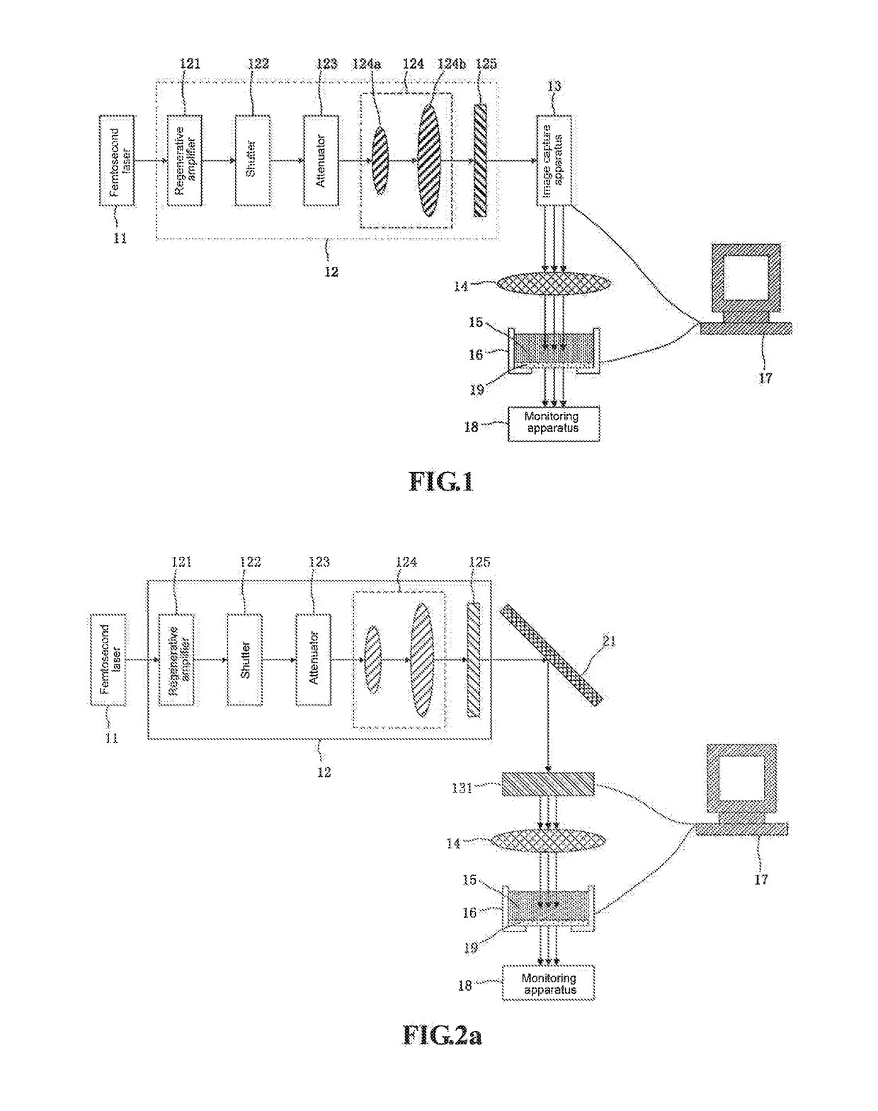
[0066]Embodiment 3 of the present disclosure also provides a system for micro-nano machining by femtosecond laser two-photon polymerization. The difference from the embodiment 2 is that the static image capture apparatus is adopted as the image capture apparatus of the present embodiment.

[0067]Further, the static image capture apparatus may be a mask plate. FIG. 4 is a schematic structural diagram illustrating the system for the micro-nano machining by femtosecond laser two-photon polymerization provided by the embodiment 3 of the present disclosure. As shown in FIG. 4, the static image capture apparatus is a mask plate 133, and in order that the structure of the whole system for the micro-nano machining is more compact, a whole reflector 21 is arranged on an advance path of femtosecond lasers and among an aperture stop 125, the mask plate 133 and an image capture apparatus 13.

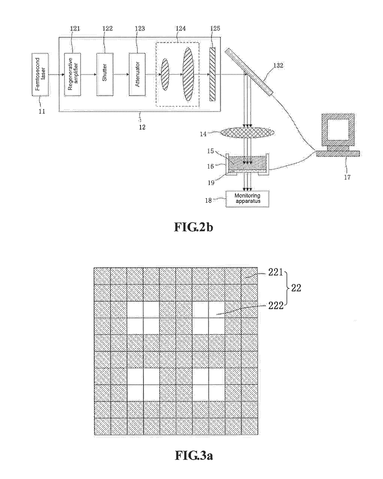
[0068]In the present embodiment, the mask plate 133 may include a plurality of microcells, where each micro...


PUM

PropertyMeasurementUnit
thicknessaaaaaaaaaa
wave lengthaaaaaaaaaa
displacementaaaaaaaaaa

Abstract

Disclosed are a system and method for micro-nano machining by femtosecond laser two-photon polymerization. The system includes: a femtosecond laser, an external light path modulation unit, an image capture apparatus, a focusing lens, a displacement platform, a computer and a monitoring apparatus, where the image capture apparatus is configured to capture cross-section graphs of a three-dimensional micro-nano device layer by layer, so that modulated femtosecond lasers form parallel beams arranged according to all layers of the cross-section graphs.

Description

[0001]The present application claims priority to a Chinese Patent application No. 201410375257.5, filed with SIPO on Aug. 1, 2014 by South University of Science and Technology of China, and entitled ‘SYSTEM AND METHOD FOR MICRO-NANO MACHINING BY FEMTOSECOND LASER TWO-PHOTON POLYMERIZATION’, the disclosure of which is incorporated herein by reference in its entirety.TECHNICAL FIELD[0002]The present disclosure relates to the technical field of micro-nano machining, and in particular relates to a system and method for micro-nano machining by femtosecond laser two-photon polymerization.BACKGROUND[0003]With the development of a semiconductor micro-electronic technology, various accompanied micro-nano machining technologies become important research contents of the modern science and technology and is widely applied in the fields of micro electromechanical systems, micro-photonic devices, precision special instruments, an information technology, biomedicine and the like.[0004]In recent ye...

Claims


Application Information

Patent Timeline
Patent Type & Authority Applications(United States)
IPC IPC(8): G03F7/20
CPCG03F7/70641G03F7/7055G03F7/0037G03F7/2053G03F7/70041G03F7/70416
Inventor CHENG, XINGCUI, DEHULI, ZIPINGMING, JING
Owner SOUTH UNIVERSITY OF SCIENCE AND TECHNOLOGY OF CHINA
Why Eureka
Try Eureka