

Structure for radio-frequency applications
- Summary
- Abstract
- Description
- Claims
- Application Information
AI Technical Summary
Benefits of technology
Problems solved by technology
Method used
Image

Examples
first embodiment
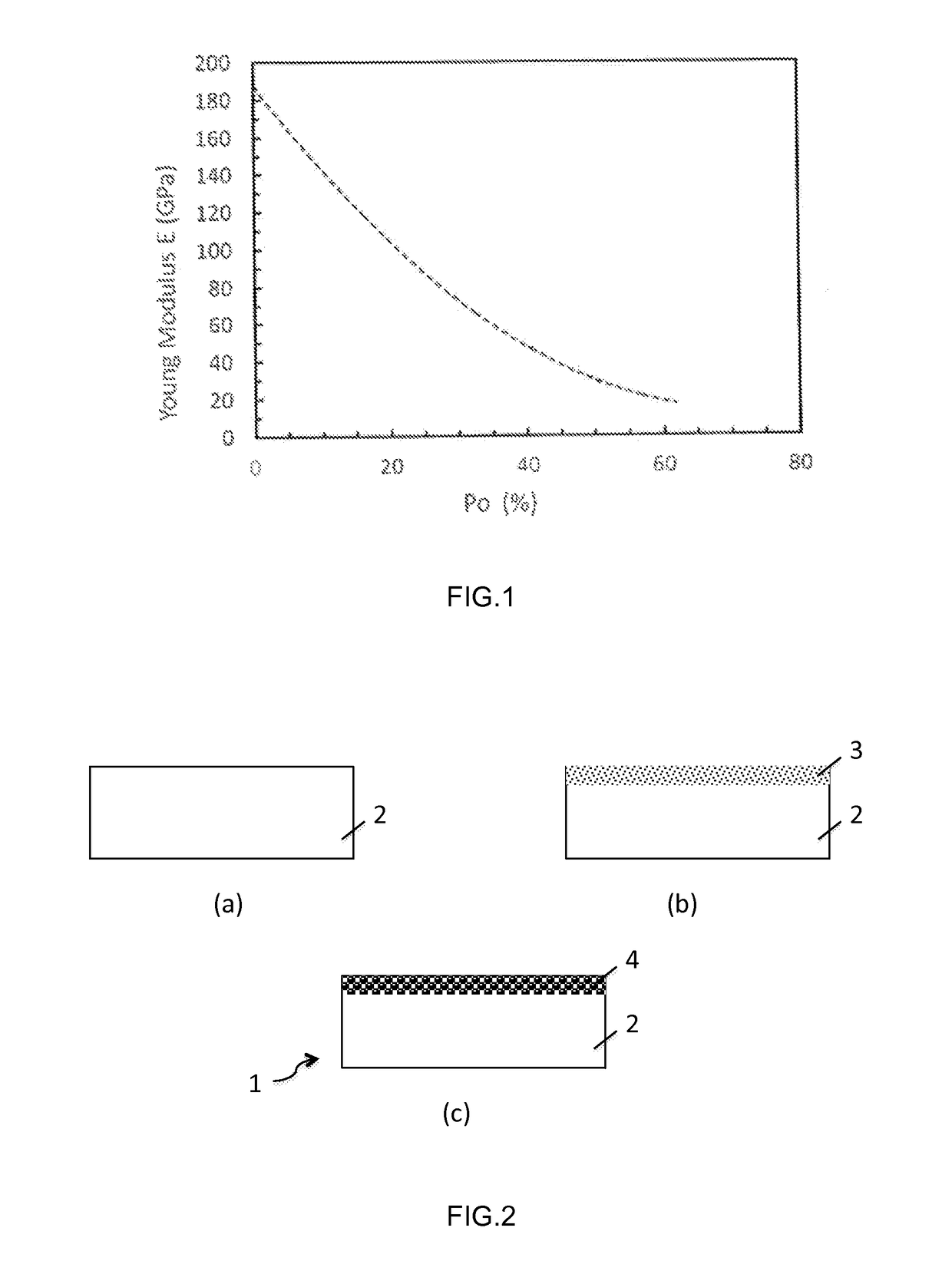
[0064]According to the disclosure represented in FIG. 2, the structure 1 for radiofrequency applications can take the form of a wafer of dimensions compatible with microelectronic processes, for example, with a diameter of 200 nm or 300 nm, comprising the support substrate 2 and the trapping layer 4 (FIG. 2, Panel (c)).
[0065]The support substrate 2 of HR silicon (FIG. 2, Panel (a)) advantageously has a resistivity greater than 4000 ohm·cm. It first of all undergoes a boron ion implantation, for example, with a dose of 1e13 / cm2 and with an energy of 50 keV, followed by a heat treatment at 1000° C. for 5 minutes; a p-doped upper part 3, to a depth of approximately 200 nm, is thus created (FIG. 2, Panel (b)). The support substrate 2 then undergoes an electrolysis: the current density will, for example, be between 10 and 20 mA / cm2 and the electrolysis solution will have an HF concentration of between 10% and 30%. The mesoporous trapping layer 4 of silicon is formed in the doped upper pa...
second embodiment
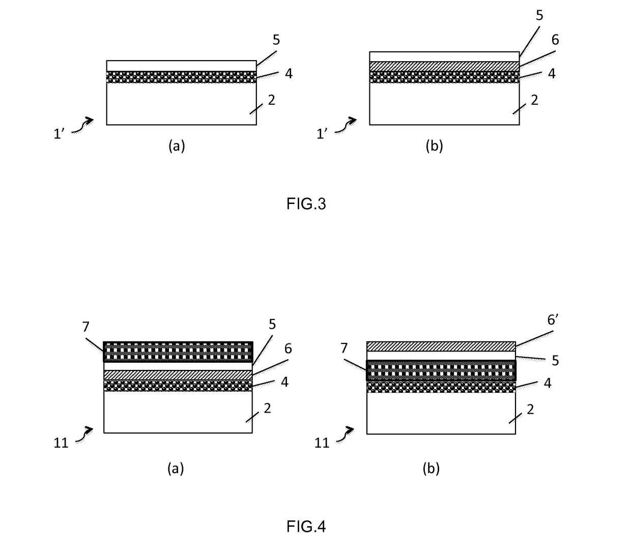
[0073]According to another variant of the second embodiment, represented in FIG. 3, Panel (b), the structure 1′ for radiofrequency applications will also be able to include a dielectric layer 6, arranged between the active layer 5 and the trapping layer 4. Advantageously, but without this being limiting, the dielectric layer 6 will comprise at least one of the materials out of: silicon dioxide, silicon nitride, aluminum oxide, etc. Its thickness will be able to vary between 10 nm and 3 μm.
[0074]The dielectric layer 6 is obtained by thermal oxidation or by LPCVD or PECVD or HDP deposition, on the trapping layer 4 or on the donor substrate prior to the transfer of the active layer 5 onto the trapping layer 4.
[0075]As is well known in the field of SOI (silicon-on-insulator) substrates for radiofrequency applications, such a dielectric layer, for example, formed by an oxide of silicon on a support substrate of silicon, comprises positive charges. These charges are compensated by negativ...
fourth embodiment
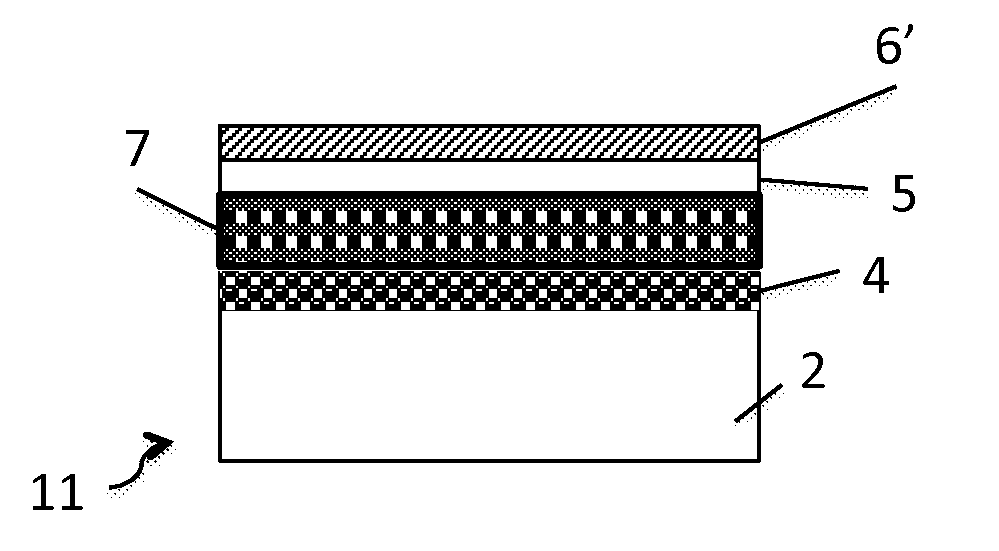
[0082] the structure 11 for radiofrequency applications can comprise or consist of a microelectronic device 7 comprising at least one control element and one MEMS (microelectromechanical system) switching element consisting of a microswitch with ohmic contact or of a capacitive microswitch.
[0083]The MEMS fabrication can be facilitated by the presence of a dielectric layer under an active layer of silicon. The structure 11 according to the disclosure will, therefore, be able to include, by way of example, an active layer 5 of silicon with a thickness of between 20 nm and 2 microns, advantageously 145 nm, and an underlying dielectric layer 6 with a thickness of between 20 nm and 1 micron, advantageously 400 nm; the trapping layer 4 is arranged between the dielectric layer 6 and the support substrate 2. The fabrication of the MEMS part is then based on surface micromachining techniques, making it possible, in particular, to free beams or mobile membranes in the active layer of silicon....
PUM
 Abstract
Description
Claims
Application Information