Secondary particle detection system of scanning electron microscope

a scanning electron microscope and detection system technology, applied in the direction of basic electric elements, electric discharge tubes, electrical equipment, etc., can solve the problems of lowering resolution, revealing the resolution limit of inspection using optical microscopes, heavy damage to devices, etc., and achieve high beam current, low damage, and high resolution

Active Publication Date: 2017-09-21
TASMIT INC
View PDF6 Cites 23 Cited by
  • Summary
  • Abstract
  • Description
  • Claims
  • Application Information

AI Technical Summary

Benefits of technology

[0044]With the upper and lower scintillators which are grounded and the Wien filter (i.e., a beam separator of EXB), the scanning electron microscope: (1) can detect secondary electrons, which have been accelerated to 6 keV to 15 keV by the retarding potential, at a high-speed pixel rate of 100 MHz or higher without causing a blur between pixels; (2) can detect almost all of the secondary electrons emitted from the specimen surface without a detection loss; and

Problems solved by technology

As microfabrication of semiconductor devices has advanced, pattern sizes have decreased less than one-several tens of a wavelength of light, thus revealing a limit of resolution in inspection using an optical microscope.
However, the high acceleration voltage results in heavier damage to devices, besides a problem of shrinkage when observing resist patterns, it has been required to observe semiconductor devices with a landing energy of 5 keV or lower.
As a result, the coulomb interaction in a beam path causes the primary beam to spread more greatly than an optical aberration, thus lowering the resolution.
The first disadvantage is that when the energy of the secondary particles (i.e., the secondary electrons and the back-scattered electrons), which enter the target plate 205, exceeds about 2 KeV, a secondary electron yield (which may to be referred to as tertiary electrons) of the target plate 205 becomes smaller than 1.
In this manner, in the target method, the process of the tertiary electron emission from the target plate 205 is a bottleneck, which hinders the method from obtaining a good SN ratio.
The second disadvantage is that, since an initial energy of the tertiary electrons generated from the target plate 205 is as low as several eV, the tertiary electrons trace variously curved trajectories depending on differences in their generation point and their take-off angle besides azimuthal angle until they reach the scintillator 206, as shown in FIG. 17.
When high-speed scanning is performed at 100 MHz, this width of the transit time is several times as long as a primary-beam dwelling time of

Method used


Image

  • Secondary particle detection system of scanning electron microscope
  • Secondary particle detection system of scanning electron microscope
  • Secondary particle detection system of scanning electron microscope

Examples


Embodiment Construction

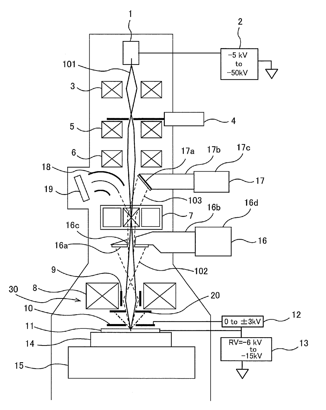
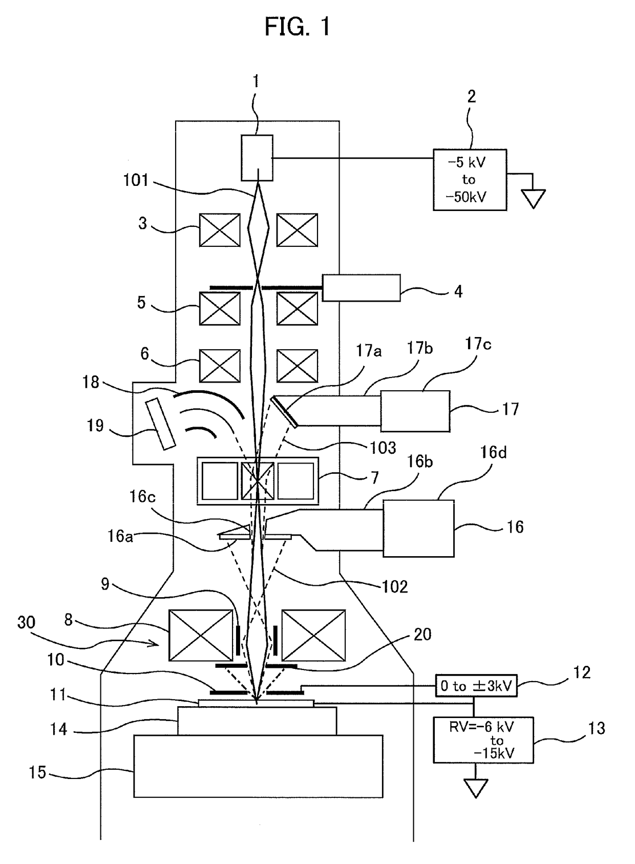
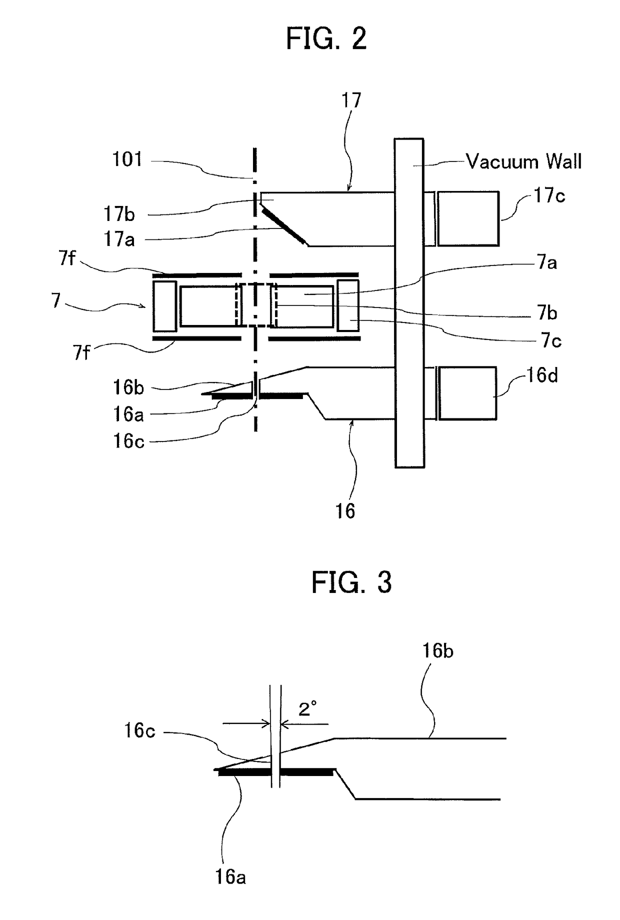
[0065]FIG. 1 is a diagram showing a whole structure of an embodiment of a scanning electron microscope (SEM) according to the present invention. As shown in FIG. 1, the scanning electron microscope includes an electron gun 1 for emitting a primary beam (or an electron beam) 101, an acceleration power source 2 for accelerating the primary beam, three condenser lenses 3, 5, 6 for converging the primary beam, a current restriction aperture 4 for restricting a beam current, a retarding power source 13 for applying a retarding voltage, which is a negative voltage, to a specimen 11 to reduce a landing energy of the primary beam, and a combined objective lens 30 for focusing the primary beam on a surface of the specimen 11.

[0066]The electron gun 1 is a TFE electron gun. The acceleration power source 2 is coupled to the electron gun 1 so that the acceleration power source 2 can apply an acceleration voltage to the electron gun 1 so as to accelerate the primary beam. The specimen 11, such as...


PUM


Abstract

A scanning electron microscope includes: a retarding power source configured to apply a retarding voltage to a specimen; a combined objective lens configured to focus the primary beam on a surface of the specimen; an electrostatic deflection system configured to deflect the primary beam to direct the primary beam to each point in a field of view on the surface of the specimen; a first scintillation detector having a first scintillator configured to emit light upon incidence of secondary electrons which have been emitted from the specimen; a Wien filter configured to deflect the secondary electrons in one direction without deflecting the primary beam; and a second scintillation detector having a second scintillator configured to detect the secondary electrons deflected by the Wien filter. The second scintillator has a distal end located away from the axis of the primary beam.

Description

BACK GROUND[0001]As microfabrication of semiconductor devices has advanced, pattern sizes have decreased less than one-several tens of a wavelength of light, thus revealing a limit of resolution in inspection using an optical microscope. A scanning electron microscope (SEM) can observe patterns with a high resolution because the wavelength of electrons is short as compared with the pattern sizes. Therefore, the scanning electron microscope has been widely used for semiconductor inspection. In recent years, however, patterns have become smaller and finer, and accordingly, a demand for the resolution of the scanning electron microscope has been increasing year by year. Furthermore, there is a demand for high-speed scanning over a large area in order to meet a requirement of a high throughput. Therefore beam current of 1 nA or more is becoming indispensable for obtaining a sufficient SN ratio in a short time.[0002]Generally, the higher an acceleration voltage for a primary beam increas...

Claims


Application Information

Patent Timeline
IPC IPC(8): H01J37/244H01J37/26H01J37/147H01J37/28
CPCH01J37/244H01J37/28H01J37/263H01J2237/2801H01J2237/103H01J2237/2448H01J37/1474H01J2237/24495H01J2237/24485
Inventor SASAKI, SUMIOTAKASHIMA, SUSUMUKATO, MAKOTOKUBOTA, KAZUFUMITANAKA, YUKIHIROYAMAZAKI, YUICHIRO
Owner TASMIT INC
Why Eureka
Try Eureka