Anodic etching of substrates

a substrate and anodized etching technology, applied in the direction of transistors, electronic switching, pulse techniques, etc., can solve the problems of lack of ac switching ability, one or more limitations of standard devices, etc., and achieve low cost, simple drive requirements, and inherent ac switching ability

Active Publication Date: 2017-10-05
WOOD JOHN
View PDF0 Cites 17 Cited by
  • Summary
  • Abstract
  • Description
  • Claims
  • Application Information

AI Technical Summary

Benefits of technology

[0013]The proposed new device can be manufactured at low cost on standard BJT fabrication equipment, has inherent AC switching ability and simple drive requirements. Voltage drop at turn on can be under 100 mV at 10's of amps per cm.sup.2 and the device can switch high voltages both on and off at will with a sing

Problems solved by technology

Whether fabricated on Silicon or a compound semiconductor such has Silicon Carbide (SiC) all these standard devices has one or more limitation

Method used


Image

  • Anodic etching of substrates
  • Anodic etching of substrates
  • Anodic etching of substrates

Examples


example conversion

of IGBT to NIGBT I2 Device

[0337]To illustrate the process of converting an IGBT to a I2 device, we took the planar IGBT example distributed with Silvaco's Atlas TCAD drift-diffusion simulator.

[0338]See http: / / www.silvaco.com / examples / tcad / section40 / example4 / for the example.

[0339]With the same doping and geometry, stripping out the MOS part and rearranging the terminals, and contacts, an I2 version reduced the simulated on-voltage from 1.75V to 0.15V at the cost of (equivalent VCE loss) 0.5V due to base current. This cost dropped to 0.2V equivalent when the lifetime was increased from 1 uS to 5 uS (still well within standard CZ wafer specifications).

[0340]The overall benefit is a 2.5-5.times. reduction of conduction losses, improvement in switching performance, a driver that can integrated on a CMOS chip, and 2 fewer manufacturing masking steps.

AC Current Conduction Paths

[0341]When considering the AC operation of an I2 device, FIG. 31 helps to visualise the main current paths in eac...

embodiments

Diode

D2-Device

[0423]The features of the method are described by way of an example, the simplest embodiment being that of an active rectifier. Externally this is a two terminal device and acts as a low-forward-voltage, high reverse blocking voltage diode. Four such devices can form a bridge-rectifier.

[0424]FIG. 37 shows the circuit and structures for producing a 2-terminal ‘diode’ device with a forward voltage of the order of 0.1V and a reverse blocking voltage of >1000V at very low leakage current. This performance contrasts with traditional high voltage silicon rectifier diodes which exhibit a forward voltage between 0.75V to 1V and cause a significant power loss especially on 120 Vac mains rectification applications (2 diodes conducting) of around 2 W per amp which equates in monetary terms to $2 per amp, per annum wasted on electricity per bridge-rectifier.

[0425]Silicon Schottky-type rectifiers are not useful at high reverse voltage because a) the reverse leakage current is very ...


PUM


Abstract

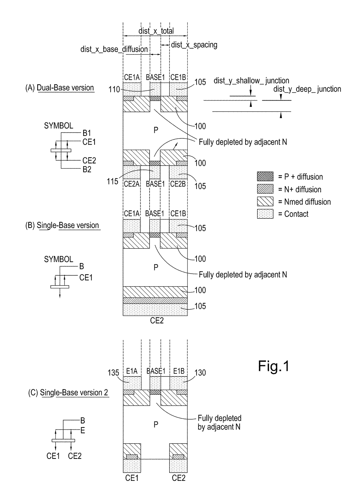
A bi-directional bipolar junction transistor (BJT) structure, comprising: a base region of a first conductivity type, wherein said base region constitutes a drift region of said structure; first and second collector/emitter (CE) regions, each of a second conductivity type adjacent opposite ends of said base region; wherein said base region is lightly doped relative to said collector/emitter regions; the structure further comprising: a base connection to said base region, wherein said base connection is within or adjacent to said first collector/emitter region.

Description

CROSS-REFERENCE OF THE RELATED APPLICATIONS[0001]This application is a continuation-in-part of U.S. patent application Ser. No. 14 / 797,498, filed Jul. 13, 2015, which is a continuation-in-part of International Application No. PCT / GB2014 / 050368 filed Feb. 7, 2014 which claims priority to United Kingdom patent application numbers GB1302196.9 filed Feb. 7, 2013, GB1305250.1 filed on Mar. 22, 2013, GB1309465.1 filed on May 27, 2013, GB1311298.2 filed on Jun. 25, 2013, GB1321151.1 filed on Nov. 29, 2013, GB1322177.5 filed on Dec. 16, 2013, GB1400866.8 filed on Jan. 20, 2014 and GB1412513.2 filed on Jul. 14, 2014, the entire disclosures of which are incorporated herein by reference in their entirety.FIELD OF THE INVENTION[0002]This invention relates to a design of semiconductor power transistor, particularly but not exclusively, to a semiconductor power switch and relays.BACKGROUND OF THE INVENTION[0003]Traditional power switches are fabricated from P and N type regions of semiconductor m...

Claims


Application Information

Patent Timeline
IPC IPC(8): H01L21/3063
CPCH01L21/3063H01L29/6625H01L29/66272H01L29/732H01L29/735H01L29/7392H01L27/0623H01L27/0705H01L29/8083H01L29/861H01L29/0804H01L29/0821H01L29/1004H03K17/665H03K17/68H01L2224/0603H01L2224/4903H01L2924/19105H01L2924/19107H01L2924/00014H01L2224/05553H01L2224/49175H01L2224/45099H01L21/306
Inventor WOOD, JOHN
Owner WOOD JOHN
Why Eureka
Try Eureka